

SN74ALVCH32245KR
Product Overview
- Category: Integrated Circuit (IC)
- Use: Level Shifter and Bus Transceiver
- Characteristics: Bi-directional voltage level translation between different logic levels, high-speed operation, low power consumption
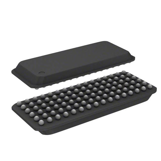
- Package: 48-pin TSSOP (Thin Shrink Small Outline Package)
- Essence: The SN74ALVCH32245KR is a level shifter and bus transceiver IC that allows for bi-directional voltage level translation between different logic levels. It is commonly used in applications where signals need to be transferred between devices operating at different voltage levels.
- Packaging/Quantity: Available in tape and reel packaging with a quantity of 2500 units per reel.
Specifications
- Supply Voltage Range: 1.2V to 3.6V
- Logic Voltage Levels: 1.2V to 3.6V
- Input/Output Compatibility: TTL, CMOS
- Number of Channels: 32
- Maximum Data Rate: 400 Mbps
- Operating Temperature Range: -40°C to +85°C
Detailed Pin Configuration
The SN74ALVCH32245KR has a total of 48 pins. The pin configuration is as follows:
- OE (Output Enable) 1B
- A1
- B1
- GND (Ground)
- B2
- A2
- 1A
- 2A
- VCC (Power Supply)
- 2B
- 1B
- OE (Output Enable) 2B
- DIR (Direction Control)
- 3A
- 4A
- GND (Ground)
- 4B
- 3B
- OE (Output Enable) 4B
- VCC (Power Supply)
- 5B
- 6B
- GND (Ground)
- 6A
- 5A
- OE (Output Enable) 6A
- DIR (Direction Control)
- 7A
- 8A
- GND (Ground)
- 8B
- 7B
- OE (Output Enable) 8B
- VCC (Power Supply)
- 9B
- 10B
- GND (Ground)
- 10A
- 9A
- OE (Output Enable) 10A
- DIR (Direction Control)
- 11A
- 12A
- GND (Ground)
- 12B
- 11B
- OE (Output Enable) 12B
- VCC (Power Supply)
Functional Features
- Bi-directional voltage level translation: Allows for seamless communication between devices operating at different logic levels.
- High-speed operation: Supports data rates of up to 400 Mbps, enabling fast and efficient data transfer.
- Low power consumption: Designed to minimize power consumption, making it suitable for battery-powered applications.
Advantages and Disadvantages
Advantages: - Enables interfacing between devices with different voltage levels. - Supports high-speed data transfer. - Low power consumption.
Disadvantages: - Requires careful consideration of voltage compatibility and signal integrity. - May introduce additional propagation delay in the signal path.
Working Principles
The SN74ALVCH32245KR operates by utilizing a combination of level shifting and bus transceiver techniques. It consists of multiple channels that can translate signals bidirectionally between two voltage domains. The direction control pin (DIR) determines the direction of data flow, while the output enable pins (OE) control the tri-state outputs. The IC is designed to provide efficient and reliable voltage level translation while minimizing power consumption.
Detailed Application Field Plans
The SN74ALVCH32245KR finds applications in various fields where voltage level translation is required. Some of the common application areas include:
- Microcontroller interfacing: It allows communication between microcontrollers operating at different logic levels.
- Memory interfaces: Enables data transfer between memory modules with different voltage requirements.
- Communication systems: Facilitates signal transmission between devices operating at different voltage levels in communication networks.
- Industrial automation: Used for interfacing sensors, actuators, and other devices with different voltage compatibility.
- Consumer electronics: Enables connectivity between devices such as smartphones, tablets, and peripherals with varying voltage levels.
Detailed and Complete Alternative Models
- TXB0108PWR: 8-bit Bidirectional Voltage-Level Translator
- PCA9306DCUR: Dual Bidirectional I2C Bus and SMBus Voltage-Level Translator
- SN74LVC4245APW:
Senaraikan 10 soalan dan jawapan biasa yang berkaitan dengan aplikasi SN74ALVCH32245KR dalam penyelesaian teknikal
Sure! Here are 10 common questions and answers related to the application of SN74ALVCH32245KR:
Q: What is SN74ALVCH32245KR? A: SN74ALVCH32245KR is a 32-bit bus transceiver with 3-state outputs, designed for low-voltage (1.65V to 3.6V) applications.
Q: What is the purpose of SN74ALVCH32245KR? A: SN74ALVCH32245KR is used to enable bidirectional level translation between two voltage domains in digital systems.
Q: What is the maximum data rate supported by SN74ALVCH32245KR? A: SN74ALVCH32245KR supports data rates up to 400 Mbps, making it suitable for high-speed applications.
Q: Can SN74ALVCH32245KR be used with different supply voltages on each side? A: Yes, SN74ALVCH32245KR can operate with different supply voltages on each side, as long as they fall within the specified range.
Q: How many channels does SN74ALVCH32245KR have? A: SN74ALVCH32245KR has 32 bidirectional channels, allowing for the simultaneous transmission of 32 bits of data.
Q: Does SN74ALVCH32245KR support hot insertion? A: Yes, SN74ALVCH32245KR is designed to support hot insertion, ensuring safe and reliable operation during system upgrades or maintenance.
Q: Can SN74ALVCH32245KR handle bus contention? A: Yes, SN74ALVCH32245KR has built-in bus-hold circuitry that prevents bus contention and reduces the possibility of data corruption.
Q: What is the output drive strength of SN74ALVCH32245KR? A: SN74ALVCH32245KR has adjustable output drive strength, allowing users to optimize it for different load conditions.
Q: Is SN74ALVCH32245KR compatible with other logic families? A: Yes, SN74ALVCH32245KR is designed to be compatible with both TTL and CMOS logic families, making it versatile in various system designs.
Q: Are there any special considerations for PCB layout when using SN74ALVCH32245KR? A: Yes, it is recommended to follow the manufacturer's guidelines for proper PCB layout, including signal integrity and decoupling capacitor placement, to ensure optimal performance.
Please note that these answers are general and may vary depending on specific application requirements. It is always advisable to refer to the datasheet and consult with the manufacturer for detailed information.