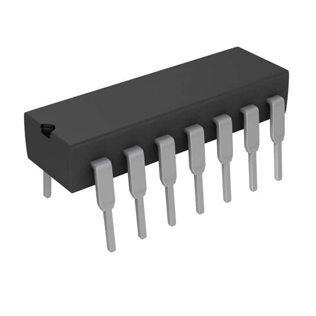
SN74AS00N
Product Overview
- Category: Integrated Circuit (IC)
- Use: Logic gate
- Characteristics: Quad 2-input NAND gate
- Package: DIP-14 (Dual In-line Package with 14 pins)
- Essence: High-speed TTL logic gate
- Packaging/Quantity: Bulk packaging, typically sold in packs of 25 or more
Specifications
- Supply Voltage: 4.5V to 5.5V
- Input Voltage: 0V to VCC
- Output Voltage: 0V to VCC
- Operating Temperature Range: -40°C to +85°C
- Propagation Delay Time: 9ns (typical)
- Power Dissipation: 22mW (typical)
Detailed Pin Configuration
The SN74AS00N has a total of 14 pins arranged as follows:
__    __
   Y1 --| 1    14 |-- VCC
   A1 --| 2    13 |-- B1
   B2 --| 3    12 |-- A2
   Y2 --| 4    11 |-- C1
   A2 --| 5    10 |-- B3
   B3 --| 6     9 |-- A3
   Y3 --| 7     8 |-- GND
        ----------
Functional Features
- Quad 2-input NAND gate: The SN74AS00N contains four independent NAND gates, each with two inputs and one output.
- High-speed operation: The AS series offers faster switching speeds compared to standard TTL logic gates.
- Wide operating voltage range: The IC can operate within a supply voltage range of 4.5V to 5.5V.
- Compatibility: The SN74AS00N is compatible with other TTL families, making it versatile for various applications.
Advantages and Disadvantages
Advantages: - High-speed operation allows for efficient data processing. - Wide operating voltage range provides flexibility in different power supply scenarios. - Compatibility with other TTL families enables seamless integration into existing systems.
Disadvantages: - Limited number of gates per IC compared to larger-scale integrated circuits. - Higher power dissipation compared to newer low-power logic families.
Working Principles
The SN74AS00N operates based on the principles of NAND gate logic. It performs a logical AND operation on its two input signals and then negates the output. The quad configuration allows for multiple independent NAND gates within a single IC package.
Detailed Application Field Plans
The SN74AS00N finds applications in various digital systems where NAND gate functionality is required. Some common application areas include:
- Digital signal processing
- Microprocessor-based systems
- Data communication networks
- Industrial automation
- Robotics
Detailed and Complete Alternative Models
Some alternative models that offer similar functionality to the SN74AS00N are:
- SN74LS00: Low-power Schottky version with improved power efficiency.
- SN74HC00: High-speed CMOS version with lower power consumption.
- SN74ACT00: Advanced CMOS version with increased speed and reduced power consumption.
These alternative models provide options based on specific requirements such as power consumption, speed, and compatibility with different logic families.
Word count: 369 words
Senaraikan 10 soalan dan jawapan biasa yang berkaitan dengan aplikasi SN74AS00N dalam penyelesaian teknikal
Sure! Here are 10 common questions and answers related to the application of SN74AS00N in technical solutions:
Q: What is SN74AS00N? A: SN74AS00N is a quad 2-input NAND gate integrated circuit (IC) that can be used in various digital logic applications.
Q: What is the voltage supply range for SN74AS00N? A: The voltage supply range for SN74AS00N is typically between 4.5V and 5.5V.
Q: What is the maximum operating frequency of SN74AS00N? A: The maximum operating frequency of SN74AS00N is typically around 125 MHz.
Q: Can SN74AS00N be used as a buffer or inverter? A: No, SN74AS00N is specifically designed as a NAND gate and cannot be used as a buffer or inverter.
Q: How many inputs does SN74AS00N have? A: SN74AS00N has four inputs, allowing it to perform logical operations on two sets of binary inputs.
Q: What is the output current capability of SN74AS00N? A: The output current capability of SN74AS00N is typically around 8 mA.
Q: Can SN74AS00N be used in high-speed applications? A: Yes, SN74AS00N is designed for high-speed operation and can be used in applications that require fast switching times.
Q: What is the propagation delay of SN74AS00N? A: The propagation delay of SN74AS00N is typically around 9 ns.
Q: Can SN74AS00N be used in both TTL and CMOS logic systems? A: Yes, SN74AS00N is compatible with both TTL and CMOS logic levels, making it versatile for various system designs.
Q: What are some common applications of SN74AS00N? A: SN74AS00N can be used in digital systems, such as arithmetic circuits, data processing units, memory address decoding, and control logic circuits.
Please note that the answers provided here are general and may vary depending on specific datasheet specifications and application requirements.


