

SN74AUC07RGYR
Product Overview
- Category: Integrated Circuit (IC)
- Use: Buffer/Driver
- Characteristics: High-speed, low-power, open-drain output
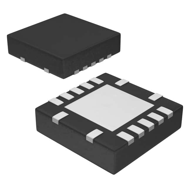
- Package: VQFN-14
- Essence: Hex buffer/driver with open-drain outputs
- Packaging/Quantity: Tape and reel, 2500 units per reel
Specifications
- Supply Voltage Range: 0.8V to 3.6V
- Input Voltage Range: -0.5V to VCC + 0.5V
- Output Voltage Range: 0V to VCC
- Maximum Operating Frequency: 500MHz
- Maximum Propagation Delay: 2.9ns
- Maximum Quiescent Current: 10μA
- Operating Temperature Range: -40°C to 85°C
Detailed Pin Configuration
The SN74AUC07RGYR has a VQFN-14 package with the following pin configuration:
- GND (Ground)
- A1 (Input A1)
- Y1 (Output Y1)
- A2 (Input A2)
- Y2 (Output Y2)
- A3 (Input A3)
- Y3 (Output Y3)
- VCC (Supply Voltage)
- A4 (Input A4)
- Y4 (Output Y4)
- A5 (Input A5)
- Y5 (Output Y5)
- A6 (Input A6)
- Y6 (Output Y6)
Functional Features
- Hex buffer/driver with open-drain outputs
- Provides buffering and driving capability for digital signals
- Open-drain outputs allow for wired-OR connections
- High-speed operation suitable for applications requiring fast signal propagation
- Low-power consumption ideal for battery-powered devices
- Wide supply voltage range allows for compatibility with various systems
Advantages and Disadvantages
Advantages: - High-speed operation enables efficient signal transmission - Low-power consumption prolongs battery life in portable devices - Open-drain outputs provide flexibility for wired-OR connections - Wide supply voltage range enhances compatibility with different systems
Disadvantages: - Limited number of buffer/driver channels (6 in this case) - Not suitable for applications requiring bidirectional communication
Working Principles
The SN74AUC07RGYR is a hex buffer/driver IC that amplifies and drives digital signals. It features open-drain outputs, which means the outputs can either be pulled low or left floating. This characteristic allows multiple devices to be connected together using a wired-OR configuration.
When an input signal is applied to one of the A inputs, the corresponding Y output will either be pulled low or remain high impedance depending on the logic level of the input. The VCC pin provides the supply voltage for the IC, while the GND pin serves as the ground reference.
Detailed Application Field Plans
The SN74AUC07RGYR is commonly used in various applications, including:
- Bus buffering: It can be used to buffer and drive signals on a bus, ensuring proper signal integrity and preventing signal degradation.
- Level shifting: It can be employed to shift the logic levels of signals between different voltage domains, allowing communication between incompatible systems.
- Wired-OR connections: The open-drain outputs make it suitable for creating wired-OR connections, where multiple devices can share a common signal line without conflicts.
- I2C communication: It can be utilized in I2C (Inter-Integrated Circuit) communication systems to provide buffering and driving capabilities for SDA and SCL lines.
Detailed and Complete Alternative Models
Some alternative models to the SN74AUC07RGYR include:
- SN74LVC07A: Similar hex buffer/driver IC with non-open-drain outputs.
- SN74HC07: Hex buffer/driver IC with open-drain outputs, but operates at higher voltage levels.
- SN74LVTH16245A: 16-bit bus transceiver with non-open-drain outputs.
These alternative models offer similar functionality but may have different specifications and pin configurations. It is important to select the appropriate model based on specific application requirements.
Word count: 511 words
Senaraikan 10 soalan dan jawapan biasa yang berkaitan dengan aplikasi SN74AUC07RGYR dalam penyelesaian teknikal
Sure! Here are 10 common questions and answers related to the application of SN74AUC07RGYR in technical solutions:
Q: What is SN74AUC07RGYR? A: SN74AUC07RGYR is a hex buffer/driver with open-drain outputs, commonly used in digital logic circuits.
Q: What is the operating voltage range for SN74AUC07RGYR? A: The operating voltage range for SN74AUC07RGYR is typically between 0.8V and 3.6V.
Q: What is the maximum output current of SN74AUC07RGYR? A: The maximum output current per channel of SN74AUC07RGYR is typically 24mA.
Q: Can SN74AUC07RGYR be used as a level shifter? A: Yes, SN74AUC07RGYR can be used as a level shifter to convert signals between different voltage levels.
Q: How many channels does SN74AUC07RGYR have? A: SN74AUC07RGYR has six independent buffer/driver channels.
Q: Is SN74AUC07RGYR suitable for high-speed applications? A: Yes, SN74AUC07RGYR is designed for high-speed operation and can be used in applications with fast switching requirements.
Q: Does SN74AUC07RGYR have built-in protection features? A: No, SN74AUC07RGYR does not have built-in protection features such as overvoltage or overcurrent protection.
Q: Can SN74AUC07RGYR drive capacitive loads? A: Yes, SN74AUC07RGYR can drive capacitive loads up to a certain limit specified in the datasheet.
Q: What is the typical propagation delay of SN74AUC07RGYR? A: The typical propagation delay of SN74AUC07RGYR is around 2.5ns.
Q: Can SN74AUC07RGYR be used in automotive applications? A: Yes, SN74AUC07RGYR is qualified for automotive applications and meets the necessary standards.
Please note that the answers provided here are general and may vary depending on specific application requirements. It's always recommended to refer to the datasheet and consult with technical experts for accurate information.