

SN74AUC2G241YEPR
Product Overview
- Category: Integrated Circuit (IC)
- Use: Logic Gate
- Characteristics: Dual Buffer/Driver with 3-State Outputs
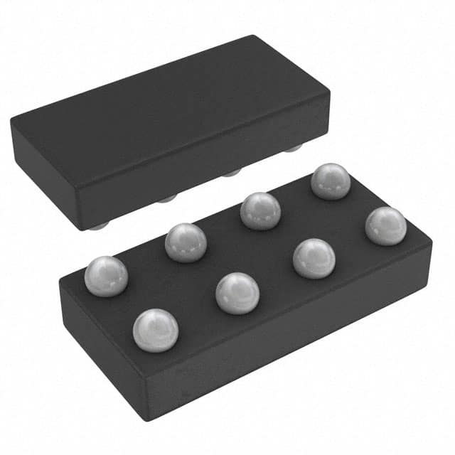
- Package: 8-pin VSSOP (Very Small Outline Package)
- Essence: This IC is designed to provide buffering and driving capabilities for digital signals in various electronic circuits.
- Packaging/Quantity: Available in tape and reel packaging, with a quantity of 3000 units per reel.
Specifications
- Supply Voltage Range: 0.8V to 3.6V
- High-Level Input Voltage: 0.7 x VCC
- Low-Level Input Voltage: 0.3 x VCC
- High-Level Output Voltage: 0.9 x VCC
- Low-Level Output Voltage: 0.1 x VCC
- Maximum Operating Frequency: 100 MHz
- Maximum Propagation Delay: 4.5 ns
- Maximum Quiescent Current: 10 µA
Detailed Pin Configuration
The SN74AUC2G241YEPR has the following pin configuration:
___________
   1 -| IN1 / OUT1 |- 8
   2 -| GND        |- 7
   3 -| IN2 / OUT2 |- 6
   4 -| OE         |- 5
       ¯¯¯¯¯¯¯¯¯¯¯
Functional Features
- Dual Buffer/Driver: The SN74AUC2G241YEPR consists of two independent buffer/driver circuits, allowing it to handle two separate input/output signals.
- 3-State Outputs: The outputs of this IC can be put into a high-impedance state using the Output Enable (OE) pin, which allows multiple devices to share a common bus without interfering with each other.
- Wide Supply Voltage Range: The IC can operate with a supply voltage ranging from 0.8V to 3.6V, making it suitable for various low-power applications.
- Fast Propagation Delay: With a maximum propagation delay of 4.5 ns, the SN74AUC2G241YEPR ensures quick signal transmission and response.
Advantages and Disadvantages
Advantages: - Low power consumption - Wide supply voltage range - High-speed operation - Small package size
Disadvantages: - Limited number of input/output channels - Relatively high cost compared to simpler logic gates
Working Principles
The SN74AUC2G241YEPR operates based on CMOS (Complementary Metal-Oxide-Semiconductor) technology. It utilizes MOSFET transistors to control the flow of current through its internal circuitry. When an input signal is applied, the buffer/driver amplifies and shapes the signal, providing a clean and reliable output.
Detailed Application Field Plans
The SN74AUC2G241YEPR is commonly used in various digital systems and electronic devices, including but not limited to: - Mobile phones - Tablets - Portable gaming consoles - Wearable devices - IoT (Internet of Things) devices - Battery-powered applications
Detailed and Complete Alternative Models
- SN74AUC2G07: Dual Buffer/Driver with Open-Drain Outputs
- SN74AUC2G125: Dual Bus Buffer Gate with 3-State Outputs
- SN74AUC2G240: Dual Inverter Buffer/Driver with 3-State Outputs
- SN74AUC2G34: Dual Buffer/Driver with Schmitt-Trigger Inputs
These alternative models offer similar functionality and characteristics to the SN74AUC2G241YEPR, providing options for different design requirements.
Word count: 430 words
Senaraikan 10 soalan dan jawapan biasa yang berkaitan dengan aplikasi SN74AUC2G241YEPR dalam penyelesaian teknikal
Sure! Here are 10 common questions and answers related to the application of SN74AUC2G241YEPR in technical solutions:
Q: What is SN74AUC2G241YEPR? A: SN74AUC2G241YEPR is a dual buffer/driver IC (integrated circuit) designed for low-voltage digital applications.
Q: What is the voltage range supported by SN74AUC2G241YEPR? A: SN74AUC2G241YEPR supports a wide voltage range from 0.8V to 3.6V, making it suitable for various low-voltage applications.
Q: What is the maximum output current of SN74AUC2G241YEPR? A: The maximum output current of SN74AUC2G241YEPR is typically around 24mA, allowing it to drive moderate loads.
Q: Can SN74AUC2G241YEPR be used as a level shifter? A: Yes, SN74AUC2G241YEPR can be used as a level shifter to convert signals between different voltage levels.
Q: Is SN74AUC2G241YEPR suitable for bidirectional communication? A: No, SN74AUC2G241YEPR is a unidirectional buffer/driver and does not support bidirectional communication.
Q: What is the propagation delay of SN74AUC2G241YEPR? A: The propagation delay of SN74AUC2G241YEPR is typically around 2.5ns, making it suitable for high-speed applications.
Q: Can SN74AUC2G241YEPR be used in battery-powered devices? A: Yes, SN74AUC2G241YEPR is designed for low-voltage applications and can be used in battery-powered devices.
Q: Does SN74AUC2G241YEPR have built-in ESD protection? A: Yes, SN74AUC2G241YEPR has built-in ESD (electrostatic discharge) protection to safeguard against static electricity damage.
Q: Can SN74AUC2G241YEPR drive capacitive loads? A: Yes, SN74AUC2G241YEPR can drive small capacitive loads typically up to 50pF without any additional components.
Q: What package options are available for SN74AUC2G241YEPR? A: SN74AUC2G241YEPR is available in various package options, including SOT-23, VSSOP, and DSBGA, providing flexibility in board design.
Please note that the answers provided here are general and may vary depending on specific datasheet specifications and application requirements.