

SN74AUP3G04RSER
Product Overview
- Category: Integrated Circuit
- Use: Logic Gate
- Characteristics: High-speed, Low-power consumption
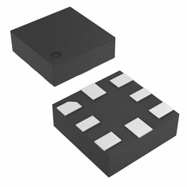
- Package: Small Outline Package (SOP)
- Essence: Inverter Gate
- Packaging/Quantity: Reel, 3000 units per reel
Specifications
- Supply Voltage Range: 0.8V to 3.6V
- Input Voltage Range: 0V to VCC
- Output Voltage Range: 0V to VCC
- Operating Temperature Range: -40°C to +85°C
- Propagation Delay: 2.5ns (typical)
Detailed Pin Configuration
The SN74AUP3G04RSER has the following pin configuration:
- GND (Ground)
- A (Input)
- Y (Output)
- VCC (Power)
Functional Features
- High-Speed Operation: The SN74AUP3G04RSER is designed for high-speed logic operations, making it suitable for applications that require fast signal processing.
- Low-Power Consumption: This integrated circuit consumes low power, making it ideal for battery-powered devices or energy-efficient systems.
- Wide Voltage Range: With a supply voltage range of 0.8V to 3.6V, the SN74AUP3G04RSER can be used in various voltage environments.
- Small Form Factor: The SOP package allows for compact and space-saving designs.
Advantages and Disadvantages
Advantages: - High-speed operation enables efficient signal processing. - Low-power consumption prolongs battery life and reduces energy costs. - Wide voltage range provides flexibility in different applications. - Small form factor allows for compact designs.
Disadvantages: - Limited number of inputs and outputs compared to larger logic gates. - May not be suitable for applications requiring complex logic operations.
Working Principles
The SN74AUP3G04RSER is an inverter gate, which means it performs the logical NOT operation. It takes an input signal and produces the complement of that signal at its output. The inverter gate consists of transistors that control the flow of current, resulting in the desired logic operation.
Detailed Application Field Plans
The SN74AUP3G04RSER can be used in various applications, including but not limited to: - Digital signal processing - Microcontrollers - Communication systems - Consumer electronics - Automotive electronics
Detailed and Complete Alternative Models
- SN74AUP1G04DCKR: Single Inverter Gate, SOT-23 package
- SN74LVC1G04DBVR: Single Inverter Gate, SOT-23 package
- SN74HC04N: Hex Inverter, DIP-14 package
- SN74LS04N: Hex Inverter, DIP-14 package
- SN74ACT04N: Hex Inverter, DIP-14 package
These alternative models offer similar functionality and can be considered as substitutes for the SN74AUP3G04RSER depending on specific requirements and design constraints.
In conclusion, the SN74AUP3G04RSER is a high-speed, low-power consumption inverter gate integrated circuit. Its small form factor and wide voltage range make it suitable for various applications in digital signal processing, microcontrollers, communication systems, consumer electronics, and automotive electronics.
Senaraikan 10 soalan dan jawapan biasa yang berkaitan dengan aplikasi SN74AUP3G04RSER dalam penyelesaian teknikal
Sure! Here are 10 common questions and answers related to the application of SN74AUP3G04RSER in technical solutions:
Q: What is SN74AUP3G04RSER? A: SN74AUP3G04RSER is a triple inverter gate IC (integrated circuit) that can be used for signal amplification, level shifting, and logic inversion.
Q: What is the voltage supply range for SN74AUP3G04RSER? A: The voltage supply range for SN74AUP3G04RSER is typically between 0.8V and 3.6V.
Q: Can SN74AUP3G04RSER be used in battery-powered applications? A: Yes, SN74AUP3G04RSER is suitable for battery-powered applications due to its low power consumption and wide voltage supply range.
Q: What is the maximum operating frequency of SN74AUP3G04RSER? A: The maximum operating frequency of SN74AUP3G04RSER is typically around 100 MHz.
Q: How many inverters are there in SN74AUP3G04RSER? A: SN74AUP3G04RSER consists of three independent inverters in a single package.
Q: Can SN74AUP3G04RSER be used as a level shifter? A: Yes, SN74AUP3G04RSER can be used as a level shifter to convert signals between different voltage levels.
Q: What is the output drive strength of SN74AUP3G04RSER? A: SN74AUP3G04RSER has a typical output drive strength of 4 mA, which allows it to drive moderate loads.
Q: Is SN74AUP3G04RSER compatible with other logic families? A: Yes, SN74AUP3G04RSER is compatible with a wide range of logic families, including CMOS, TTL, and LVCMOS.
Q: Can SN74AUP3G04RSER be used in high-temperature environments? A: SN74AUP3G04RSER has a maximum operating temperature of 125°C, making it suitable for many high-temperature applications.
Q: What is the package type of SN74AUP3G04RSER? A: SN74AUP3G04RSER is available in a small SOT-23 package, which is commonly used for surface-mount applications.
Please note that the answers provided here are general and may vary depending on specific datasheet specifications and application requirements.