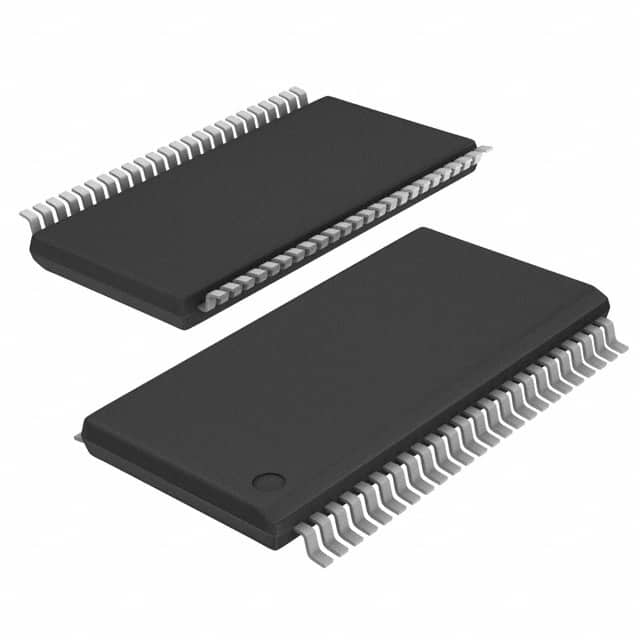
SN74CBT16209ADGVR
Product Overview
- Category: Integrated Circuit (IC)
- Use: Digital Multiplexer/Demultiplexer
- Characteristics: High-speed, low-power consumption
- Package: VSSOP-56
- Essence: 16-bit bus switch with 3-state outputs
- Packaging/Quantity: Tape and Reel, 2500 units per reel
Specifications
- Number of Channels: 16
- Input Voltage Range: 0V to VCC
- Output Voltage Range: 0V to VCC
- Supply Voltage Range: 1.65V to 3.6V
- Operating Temperature Range: -40°C to 85°C
- On-State Resistance: 5Ω (typical)
- Bandwidth: 400MHz (typical)
Detailed Pin Configuration
The SN74CBT16209ADGVR has a total of 56 pins, which are distributed as follows:
- Pin 1: OE (Output Enable)
- Pins 2-17: A0-A15 (Address Inputs)
- Pins 18-33: B0-B15 (Data Bus Inputs/Outputs)
- Pins 34-49: C0-C15 (Data Bus Inputs/Outputs)
- Pins 50-55: GND (Ground)
- Pin 56: VCC (Supply Voltage)
Functional Features
- 16-bit bidirectional switching capability
- 3-state outputs for bus sharing
- Low power consumption
- Fast switching speed
- Wide operating voltage range
Advantages and Disadvantages
Advantages: - High-speed operation allows for efficient data transfer - Low power consumption helps in reducing energy usage - 3-state outputs enable bus sharing, optimizing resource utilization - Wide operating voltage range provides flexibility in various applications
Disadvantages: - Limited number of channels (16) - On-state resistance may affect signal integrity in certain scenarios
Working Principles
The SN74CBT16209ADGVR is a digital multiplexer/demultiplexer IC that allows for bidirectional switching of a 16-bit data bus. It features 3-state outputs, which enable multiple devices to share the same bus without interfering with each other.
The IC operates by controlling the OE pin, which enables or disables the output drivers. When the OE pin is high, the outputs are in a high-impedance state, allowing other devices to drive the bus. When the OE pin is low, the outputs mirror the inputs, either transmitting data from the A-side to the B-side or vice versa.
Detailed Application Field Plans
The SN74CBT16209ADGVR is commonly used in various applications, including:
- Data communication systems: The IC facilitates efficient data transfer between different components in communication systems, such as routers, switches, and network interfaces.
- Memory modules: It can be utilized in memory modules to enable multiplexing and demultiplexing of data buses, optimizing memory access and utilization.
- Test and measurement equipment: The IC is suitable for use in test and measurement instruments, where it helps in routing signals and managing data flow between different sections of the equipment.
- Industrial automation: It finds application in industrial automation systems, enabling efficient data exchange between sensors, actuators, and control units.
- Automotive electronics: The IC can be employed in automotive electronics for various purposes, including bus sharing, data routing, and signal conditioning.
Detailed and Complete Alternative Models
- SN74CBT16210: Similar to SN74CBT16209ADGVR but with 20 channels instead of 16.
- SN74CBT3257: 8-channel analog switch with 3-state outputs.
- SN74CBT3384: 10-bit bus switch with 3-state outputs and hot insertion capability.
These alternative models offer similar functionality to the SN74CBT16209ADGVR but may have different specifications or pin configurations, providing options for specific application requirements.
Word count: 460 words
Senaraikan 10 soalan dan jawapan biasa yang berkaitan dengan aplikasi SN74CBT16209ADGVR dalam penyelesaian teknikal
Sure! Here are 10 common questions and answers related to the application of SN74CBT16209ADGVR:
Question: What is the SN74CBT16209ADGVR?
Answer: The SN74CBT16209ADGVR is a 24-bit FET bus switch designed for high-speed digital applications.Question: What is the maximum operating voltage of the SN74CBT16209ADGVR?
Answer: The maximum operating voltage is 3.6V.Question: What is the typical on-state resistance of the SN74CBT16209ADGVR?
Answer: The typical on-state resistance is 5 ohms.Question: Can the SN74CBT16209ADGVR be used for bidirectional communication?
Answer: Yes, it can be used for bidirectional communication as it supports both input and output signals.Question: What is the maximum data rate supported by the SN74CBT16209ADGVR?
Answer: The maximum data rate is 400 Mbps.Question: Does the SN74CBT16209ADGVR have built-in ESD protection?
Answer: Yes, it has built-in ESD protection, making it suitable for robust applications.Question: Can the SN74CBT16209ADGVR be cascaded to increase the number of channels?
Answer: Yes, multiple SN74CBT16209ADGVR devices can be cascaded to increase the number of channels.Question: What is the power supply range for the SN74CBT16209ADGVR?
Answer: The power supply range is from 1.65V to 3.6V.Question: Is the SN74CBT16209ADGVR compatible with both CMOS and TTL logic levels?
Answer: Yes, it is compatible with both CMOS and TTL logic levels.Question: Can the SN74CBT16209ADGVR be used in automotive applications?
Answer: Yes, the SN74CBT16209ADGVR is AEC-Q100 qualified, making it suitable for automotive applications.
Please note that these answers are general and may vary depending on the specific requirements and use cases. It's always recommended to refer to the datasheet and consult the manufacturer for detailed information.


