

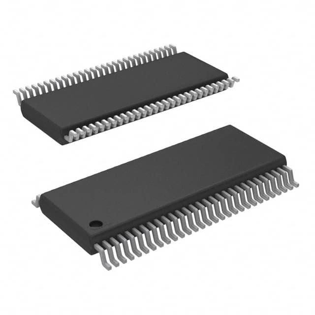
SN74CBT16811CDGVR
Product Overview
- Category: Integrated Circuit (IC)
- Use: Digital Multiplexer/Demultiplexer
- Characteristics: High-speed, low-power consumption
- Package: VFBGA (Very Fine Pitch Ball Grid Array)
- Essence: A versatile IC used for digital signal routing and control
- Packaging/Quantity: Tape and Reel, 2500 units per reel
Specifications
- Number of Channels: 24
- Input Voltage Range: 0V to VCC
- Supply Voltage Range: 1.65V to 3.6V
- On-State Resistance: 5Ω (typical)
- Bandwidth: 400MHz (typical)
- Operating Temperature Range: -40°C to +85°C
Detailed Pin Configuration
The SN74CBT16811CDGVR has a total of 56 pins. The pin configuration is as follows:
- OE (Output Enable) 1
- I/O0 (Input/Output) 1
- I/O1
- I/O2
- I/O3
- I/O4
- I/O5
- GND (Ground)
- I/O6
- I/O7
- I/O8
- I/O9
- I/O10
- I/O11
- VCC (Supply Voltage)
- I/O12
- I/O13
- I/O14
- I/O15
- I/O16
- I/O17
- I/O18
- I/O19
- I/O20
- I/O21
- I/O22
- I/O23
- OE (Output Enable) 2
- GND (Ground)
- I/O24
- I/O25
- I/O26
- I/O27
- I/O28
- I/O29
- VCC (Supply Voltage)
- I/O30
- I/O31
- I/O32
- I/O33
- I/O34
- I/O35
- GND (Ground)
- I/O36
- I/O37
- I/O38
- I/O39
- I/O40
- I/O41
- I/O42
- I/O43
- I/O44
- I/O45
- I/O46
- I/O47
- OE (Output Enable) 3
Functional Features
- High-speed switching capability for efficient signal routing
- Low power consumption for energy-efficient operation
- Wide input voltage range allows compatibility with various digital systems
- On-state resistance ensures minimal signal distortion
- Multiple channels enable versatile signal routing options
Advantages and Disadvantages
Advantages: - High-speed operation enables efficient data transmission - Low power consumption reduces energy costs - Versatile channel configuration provides flexibility in signal routing - Wide input voltage range ensures compatibility with different systems
Disadvantages: - Limited number of channels may not be suitable for applications requiring a higher channel count - On-state resistance may introduce slight signal degradation
Working Principles
The SN74CBT16811CDGVR is a digital multiplexer/demultiplexer IC that operates by selectively connecting one of the multiple input/output channels to the common output/input line based on the control signals. It utilizes CMOS technology to achieve high-speed switching while consuming low power. The IC's internal circuitry consists of transmission gates that control the signal flow between the input and output channels.
Detailed Application Field Plans
The SN74CBT16811CDGVR finds applications in various fields, including:
- Data communication systems: Used for signal routing in high-speed data transmission systems, such as Ethernet switches and routers.
- Test and measurement equipment: Enables efficient signal switching and control in test and measurement setups, ensuring accurate measurements.
- Audio/video equipment: Facilitates signal routing in audio/video switchers, allowing seamless switching between different sources.
- Industrial automation: Used in control systems to route digital signals between different components, enhancing automation processes.
- Automotive electronics: Enables signal routing in automotive systems, such as infotainment systems and instrument clusters.
Detailed and Complete Alternative Models
- SN74CBT3257CDBQR
- SN74CBT16212ADGGR
- SN74CBT3384ADBQR
- SN74CBT3257CPWR
- SN74CBT16245DLR
These alternative models offer similar functionality and characteristics to the SN74CBT16811CDGVR, providing
Senaraikan 10 soalan dan jawapan biasa yang berkaitan dengan aplikasi SN74CBT16811CDGVR dalam penyelesaian teknikal
Sure! Here are 10 common questions and answers related to the application of SN74CBT16811CDGVR:
Q: What is SN74CBT16811CDGVR? A: SN74CBT16811CDGVR is a high-performance, 24-bit bus switch with integrated level shifting capabilities.
Q: What is the voltage range supported by SN74CBT16811CDGVR? A: SN74CBT16811CDGVR supports a voltage range from 1.2V to 3.6V.
Q: Can SN74CBT16811CDGVR be used for bidirectional level shifting? A: Yes, SN74CBT16811CDGVR can be used for bidirectional level shifting between different voltage domains.
Q: What is the maximum data rate supported by SN74CBT16811CDGVR? A: SN74CBT16811CDGVR supports a maximum data rate of 100 Mbps.
Q: How many channels does SN74CBT16811CDGVR have? A: SN74CBT16811CDGVR has 24 channels, allowing for simultaneous switching of multiple signals.
Q: Can SN74CBT16811CDGVR be used in hot-swapping applications? A: Yes, SN74CBT16811CDGVR supports hot-swapping, making it suitable for applications where devices need to be plugged/unplugged while powered on.
Q: Does SN74CBT16811CDGVR have built-in ESD protection? A: Yes, SN74CBT16811CDGVR has built-in ESD protection, ensuring robustness against electrostatic discharge events.
Q: What is the power supply voltage range for SN74CBT16811CDGVR? A: SN74CBT16811CDGVR operates with a power supply voltage range from 1.65V to 3.6V.
Q: Can SN74CBT16811CDGVR be used in both digital and analog applications? A: Yes, SN74CBT16811CDGVR can be used in both digital and analog applications, thanks to its low ON-state resistance and low crosstalk.
Q: Is SN74CBT16811CDGVR available in different package options? A: Yes, SN74CBT16811CDGVR is available in various package options, including VSSOP and TSSOP, providing flexibility for different PCB layouts.
Please note that these answers are general and may vary depending on specific application requirements. It's always recommended to refer to the datasheet and consult with the manufacturer for detailed information.