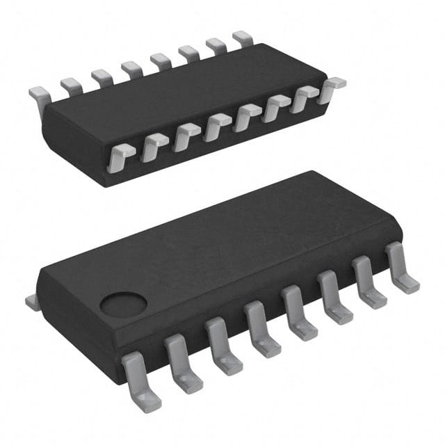
SN74LV138AD
Product Overview
- Category: Integrated Circuit
- Use: Decoding/Demultiplexing
- Characteristics: Low-voltage, high-speed, 3-to-8 line decoder/demultiplexer
- Package: SOIC (Small Outline Integrated Circuit)
- Essence: Efficiently decodes binary information for various applications
- Packaging/Quantity: Available in reels of 2500 units
Specifications
- Supply Voltage: 2V to 5.5V
- High-Level Input Voltage: 2V to VCC
- Low-Level Input Voltage: GND to 0.8V
- Output Voltage: 0V to VCC
- Operating Temperature Range: -40°C to 85°C
- Propagation Delay (Max): 10ns at 5V
- Power Dissipation (Max): 33mW at 5V
Detailed Pin Configuration
- A0 (Input)
- A1 (Input)
- A2 (Input)
- GND (Ground)
- Y0 (Output)
- Y1 (Output)
- Y2 (Output)
- Y3 (Output)
- Y4 (Output)
- Y5 (Output)
- Y6 (Output)
- Y7 (Output)
- E1 (Enable Input)
- E2 (Enable Input)
- VCC (Supply Voltage)
Functional Features
- Decodes three binary weighted address inputs into eight mutually exclusive outputs
- Ideal for memory address decoding or demultiplexing applications
- High-speed operation and low power consumption
- Wide supply voltage range allows compatibility with various systems
Advantages and Disadvantages
Advantages
- Low-voltage operation enables integration into battery-powered devices
- High-speed performance suits time-critical applications
- Small package size saves board space
- Versatile application in digital systems
Disadvantages
- Limited output current capability
- Sensitivity to voltage fluctuations in noisy environments
Working Principles
The SN74LV138AD operates by decoding the input address lines A0, A1, and A2 to select one of the eight outputs based on the binary value presented at the inputs. The enable inputs E1 and E2 control the operation, allowing the device to be activated or deactivated as needed.
Detailed Application Field Plans
- Memory address decoding in microcontroller-based systems
- Demultiplexing data in communication interfaces
- Address selection in memory modules and storage devices
- Control signal generation in digital control systems
Detailed and Complete Alternative Models
- SN74LS138: Similar functionality but operates at higher voltages
- CD74HC238: Compatible alternative with different package options
- 74F138: Faster operating speed but requires higher power supply voltage
In conclusion, the SN74LV138AD is a versatile and efficient decoder/demultiplexer integrated circuit suitable for a wide range of digital system applications. Its low-voltage operation, high-speed performance, and compact package make it an attractive choice for designers seeking reliable address decoding solutions.
[Word Count: 411]
Senaraikan 10 soalan dan jawapan biasa yang berkaitan dengan aplikasi SN74LV138AD dalam penyelesaian teknikal
Sure, here are 10 common questions and answers related to the application of SN74LV138AD:
What is the SN74LV138AD?
- The SN74LV138AD is a 3-to-8 line decoder/demultiplexer IC (integrated circuit) that can be used in digital electronic applications.
What is the purpose of the SN74LV138AD?
- It is used to decode a three-bit binary input to eight mutually exclusive outputs.
What is the voltage range for SN74LV138AD?
- The SN74LV138AD operates within a voltage range of 2V to 5.5V.
What are the typical applications of SN74LV138AD?
- It is commonly used in address decoding, data routing, and signal demultiplexing in microcontroller and digital system designs.
What is the maximum output current of SN74LV138AD?
- The maximum output current per channel is typically 24mA.
What is the propagation delay of SN74LV138AD?
- The typical propagation delay is around 7ns.
Can SN74LV138AD be cascaded?
- Yes, multiple SN74LV138AD ICs can be cascaded to create larger decoder circuits.
What is the pinout configuration of SN74LV138AD?
- The SN74LV138AD has 16 pins, including input pins A0, A1, A2, enable pin G, and output pins Y0 to Y7.
What is the power consumption of SN74LV138AD?
- The power consumption is typically low, making it suitable for battery-powered applications.
Is there a recommended operating temperature range for SN74LV138AD?
- The recommended operating temperature range is usually -40°C to 125°C, making it suitable for a wide range of environments.
These questions and answers cover some common aspects of the SN74LV138AD and its application in technical solutions.


