

SN74LV174ADGVR
Product Overview
Category
SN74LV174ADGVR belongs to the category of integrated circuits (ICs).
Use
It is commonly used in electronic devices for signal processing and control.
Characteristics
- Low-voltage operation
- High-speed performance
- Wide operating temperature range
- Small package size
- Low power consumption
Package
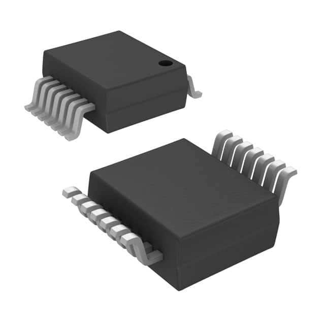
SN74LV174ADGVR is available in a small form factor package, typically a VSSOP (Very Small Outline Package).
Essence
The essence of SN74LV174ADGVR lies in its ability to process and manipulate digital signals efficiently.
Packaging/Quantity
SN74LV174ADGVR is usually packaged in reels or tubes, with a typical quantity of 2500 units per reel/tube.
Specifications
- Supply Voltage: 2.0V to 5.5V
- Logic Family: LV (Low Voltage)
- Number of Flip-Flops: 6
- Input/Output Compatibility: CMOS/TTL
- Operating Temperature Range: -40°C to +85°C
- Propagation Delay: <10ns
Detailed Pin Configuration
- CLR (Clear) - Clear input for resetting the flip-flop outputs.
- D (Data) - Input for setting the flip-flop outputs.
- CP (Clock Pulse) - Input for clocking the flip-flop outputs.
- Q0-Q5 (Flip-Flop Outputs) - Outputs representing the state of each flip-flop.
- GND (Ground) - Ground reference for the IC.
- VCC (Supply Voltage) - Positive supply voltage for the IC.
Functional Features
- Asynchronous clear input for easy reset of flip-flop outputs.
- Positive-edge triggered clock input for synchronized operation.
- High-speed operation for efficient signal processing.
- Low power consumption for energy-efficient designs.
- Wide operating temperature range for versatile applications.
Advantages and Disadvantages
Advantages
- Low-voltage operation allows compatibility with a wide range of systems.
- High-speed performance enables efficient signal processing.
- Small package size saves board space in compact designs.
- Low power consumption contributes to energy efficiency.
Disadvantages
- Limited number of flip-flops may restrict the complexity of certain applications.
- CMOS/TTL input/output compatibility may require level shifting in some cases.
Working Principles
SN74LV174ADGVR is based on the principles of digital logic circuits. It utilizes flip-flops to store and manipulate binary information. The clock pulse triggers the flip-flops, while the data input sets their outputs. The clear input allows for resetting the flip-flop outputs when necessary.
Detailed Application Field Plans
SN74LV174ADGVR finds applications in various fields, including: 1. Communication systems 2. Consumer electronics 3. Industrial automation 4. Automotive electronics 5. Medical devices
In communication systems, it can be used for data synchronization and signal processing. In consumer electronics, it can be employed in remote controls and audio/video equipment. In industrial automation, it can facilitate control and monitoring tasks. In automotive electronics, it can contribute to vehicle control systems. In medical devices, it can assist in data acquisition and processing.
Detailed and Complete Alternative Models
Some alternative models that offer similar functionality to SN74LV174ADGVR are: 1. 74HC174 - High-speed CMOS logic IC with similar pin configuration. 2. CD40174 - CMOS hex D-type flip-flop IC with comparable characteristics. 3. MC74LVX174 - Low-voltage CMOS logic IC with six D-type flip-flops.
These alternative models can be considered based on specific requirements and availability.
Word count: 526 words
Senaraikan 10 soalan dan jawapan biasa yang berkaitan dengan aplikasi SN74LV174ADGVR dalam penyelesaian teknikal
Sure! Here are 10 common questions and answers related to the application of SN74LV174ADGVR:
Q: What is the SN74LV174ADGVR? A: The SN74LV174ADGVR is a hex D-type flip-flop with clear, designed for use in various digital applications.
Q: What is the operating voltage range of SN74LV174ADGVR? A: The operating voltage range of SN74LV174ADGVR is from 2 V to 5.5 V.
Q: How many flip-flops are there in SN74LV174ADGVR? A: SN74LV174ADGVR consists of six individual D-type flip-flops.
Q: What is the maximum clock frequency supported by SN74LV174ADGVR? A: The maximum clock frequency supported by SN74LV174ADGVR is typically 125 MHz.
Q: Can SN74LV174ADGVR be used in both synchronous and asynchronous applications? A: Yes, SN74LV174ADGVR can be used in both synchronous and asynchronous applications.
Q: Does SN74LV174ADGVR have a clear input? A: Yes, SN74LV174ADGVR has an asynchronous clear input that resets all flip-flops to a low state.
Q: What is the output drive capability of SN74LV174ADGVR? A: SN74LV174ADGVR has a typical output drive capability of ±24 mA.
Q: Can SN74LV174ADGVR tolerate overvoltage on its inputs? A: No, SN74LV174ADGVR is not designed to tolerate overvoltage on its inputs. It is recommended to stay within the specified voltage range.
Q: What is the power supply current consumption of SN74LV174ADGVR? A: The power supply current consumption of SN74LV174ADGVR depends on the operating conditions and can be found in the datasheet.
Q: Can SN74LV174ADGVR be used in automotive applications? A: Yes, SN74LV174ADGVR is qualified for automotive applications and meets the necessary standards.
Please note that these answers are general and it's always recommended to refer to the datasheet and application notes for specific details and guidelines.