

SN74LVC02ARGYR
Product Overview
- Category: Integrated Circuit (IC)
- Use: Logic Gate
- Characteristics: Low Voltage CMOS Quad 2-Input NOR Gate
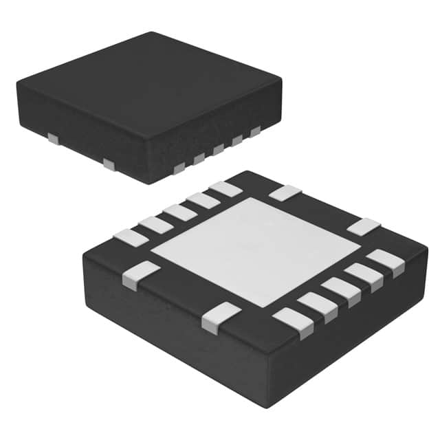
- Package: VQFN-14
- Essence: This IC is a quad 2-input NOR gate that operates at low voltage levels.
- Packaging/Quantity: Tape and Reel, 2500 pieces per reel
Specifications
- Supply Voltage Range: 1.65V to 5.5V
- High-Level Input Voltage: 2V to VCC + 0.5V
- Low-Level Input Voltage: -0.5V to 0.8V
- High-Level Output Voltage: VCC - 0.5V
- Low-Level Output Voltage: 0.5V
- Maximum Operating Frequency: 100MHz
- Propagation Delay: 3.7ns (Max) at 3.3V
- Operating Temperature Range: -40°C to 85°C
Detailed Pin Configuration
The SN74LVC02ARGYR has a VQFN-14 package with the following pin configuration:
``` __ __ |1 \/ 14| A1|2 13|VCC A2|3 12|B2 Y1|4 11|A3 Y2|5 10|B3 GND|6 9|Y3 B1|7 8|Y4
```
Functional Features
- Quad 2-input NOR gate functionality
- Low voltage operation suitable for battery-powered devices
- Compatible with TTL and CMOS logic levels
- Schmitt-trigger input allows for noisy signal rejection
- Balanced propagation delays ensure glitch-free operation
- High-speed operation with low power consumption
Advantages and Disadvantages
Advantages: - Low voltage operation extends battery life - Wide supply voltage range allows for compatibility with various systems - Schmitt-trigger input enhances noise immunity - Fast propagation delay enables high-speed applications - Small package size saves board space
Disadvantages: - Limited number of inputs (only 2 per gate) - Not suitable for high-power applications - May require additional components for certain circuit configurations
Working Principles
The SN74LVC02ARGYR is a quad 2-input NOR gate that operates using CMOS technology. It accepts two logic inputs, A and B, and provides an output, Y, based on the NOR gate truth table. The IC operates at low voltage levels, making it suitable for battery-powered devices.
The Schmitt-trigger input ensures reliable operation even in the presence of noisy signals. The balanced propagation delays between inputs and outputs prevent glitches and ensure stable logic levels. The IC is compatible with both TTL and CMOS logic levels, allowing for easy integration into existing systems.
Detailed Application Field Plans
The SN74LVC02ARGYR can be used in various applications, including:
- Battery-powered devices: The low voltage operation makes it ideal for portable electronics such as smartphones, tablets, and wearables.
- Industrial control systems: The IC can be used in logic circuits for controlling machinery, sensors, and actuators.
- Automotive electronics: It can be employed in automotive control units, dashboard displays, and infotainment systems.
- Communication systems: The IC can be utilized in signal processing circuits, data transmission, and networking equipment.
- Consumer electronics: It finds applications in TVs, set-top boxes, gaming consoles, and home appliances.
Detailed and Complete Alternative Models
- SN74LVC02APWR: TSSOP-14 package, same functionality as SN74LVC02ARGYR.
- MC74VHC02DT: TSSOP-14 package, quad 2-input NOR gate with similar specifications.
- CD4001BM96: SOIC-14 package, quad 2-input NOR gate with comparable characteristics.
These alternative models provide similar functionality and can be used as replacements for the SN74LVC02ARGYR in various applications.
Word count: 518 words
Senaraikan 10 soalan dan jawapan biasa yang berkaitan dengan aplikasi SN74LVC02ARGYR dalam penyelesaian teknikal
Sure! Here are 10 common questions and answers related to the application of SN74LVC02ARGYR:
1. What is SN74LVC02ARGYR? SN74LVC02ARGYR is a quad 2-input NOR gate IC (integrated circuit) that is commonly used in digital logic circuits.
2. What is the operating voltage range of SN74LVC02ARGYR? The operating voltage range of SN74LVC02ARGYR is from 1.65V to 5.5V.
3. What is the maximum output current of SN74LVC02ARGYR? The maximum output current of SN74LVC02ARGYR is 32mA.
4. Can SN74LVC02ARGYR be used in both CMOS and TTL logic systems? Yes, SN74LVC02ARGYR is compatible with both CMOS and TTL logic systems.
5. What is the typical propagation delay of SN74LVC02ARGYR? The typical propagation delay of SN74LVC02ARGYR is around 3.8ns.
6. Can SN74LVC02ARGYR be used for level shifting applications? Yes, SN74LVC02ARGYR can be used for level shifting applications as it supports voltage translation between different logic levels.
7. Is SN74LVC02ARGYR suitable for high-speed applications? Yes, SN74LVC02ARGYR is suitable for high-speed applications due to its low propagation delay and high-speed operation.
8. Does SN74LVC02ARGYR have built-in protection features? Yes, SN74LVC02ARGYR has built-in ESD (electrostatic discharge) protection features to prevent damage from static electricity.
9. Can SN74LVC02ARGYR be used in automotive applications? Yes, SN74LVC02ARGYR is qualified for automotive applications and meets the AEC-Q100 standard.
10. What is the package type of SN74LVC02ARGYR? SN74LVC02ARGYR is available in a small-outline integrated circuit (SOIC) package with 14 pins.
Please note that these answers are general and may vary depending on the specific datasheet and manufacturer's specifications of SN74LVC02ARGYR.