

SN74LVC112ADGVR
Overview
Category: Integrated Circuit (IC)
Use: Digital Logic Gate
Characteristics: - Low-voltage CMOS technology - Dual negative-edge-triggered JK flip-flop - Schmitt-trigger inputs for noise immunity - High-speed operation - Wide operating voltage range - Low power consumption
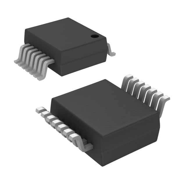
Package: VSSOP-8
Essence: The SN74LVC112ADGVR is a dual negative-edge-triggered JK flip-flop integrated circuit. It is designed using low-voltage CMOS technology, providing high-speed operation and low power consumption.
Packaging/Quantity: The SN74LVC112ADGVR is available in a VSSOP-8 package. It is typically sold in reels of 2500 units.
Specifications
- Supply Voltage Range: 1.65V to 5.5V
- Input Voltage Range: -0.5V to VCC + 0.5V
- Output Voltage Range: 0V to VCC
- Operating Temperature Range: -40°C to 85°C
- Maximum Propagation Delay: 4.3 ns
- Maximum Operating Frequency: 100 MHz
Pin Configuration
The SN74LVC112ADGVR has the following pin configuration:
__    __
   Q1 |1  \/  8| VCC
   J1 |2      7| Q2
   K1 |3      6| K2
  GND |4      5| J2
       --------
Functional Features
- Dual negative-edge-triggered JK flip-flop with independent J, K, clock (CLK), and reset (CLR) inputs.
- Schmitt-trigger inputs provide improved noise immunity.
- Outputs (Q1 and Q2) change state on the falling edge of the clock signal.
- Asynchronous reset (CLR) clears both flip-flops to a low output state.
Advantages
- Low-voltage operation allows compatibility with a wide range of systems.
- High-speed operation enables efficient data processing.
- Schmitt-trigger inputs provide noise immunity, ensuring reliable operation in noisy environments.
- Small package size (VSSOP-8) saves board space.
Disadvantages
- Limited number of flip-flops (dual) compared to other ICs with more flip-flops.
- Not suitable for high-voltage applications due to the specified supply voltage range.
Working Principles
The SN74LVC112ADGVR consists of two independent JK flip-flops. Each flip-flop has J, K, CLK, and CLR inputs. The outputs (Q1 and Q2) change state on the falling edge of the CLK signal. The CLR input asynchronously clears both flip-flops to a low output state.
Application Field Plans
The SN74LVC112ADGVR is commonly used in various digital logic applications, including:
- Sequential logic circuits
- State machines
- Data storage and transfer systems
- Clock synchronization circuits
- Control systems
Alternative Models
Some alternative models that can be considered as replacements for the SN74LVC112ADGVR are:
- CD4013BE: Dual D-type flip-flop
- 74HC112: Dual negative-edge-triggered JK flip-flop
- MC74LVX112: Dual negative-edge-triggered JK flip-flop with Schmitt-trigger inputs
These alternative models offer similar functionality and can be used as drop-in replacements in many applications.
In conclusion, the SN74LVC112ADGVR is a dual negative-edge-triggered JK flip-flop integrated circuit. It offers high-speed operation, low power consumption, and noise immunity. It is commonly used in various digital logic applications and has alternative models available for substitution.
Senaraikan 10 soalan dan jawapan biasa yang berkaitan dengan aplikasi SN74LVC112ADGVR dalam penyelesaian teknikal
Sure! Here are 10 common questions and answers related to the application of SN74LVC112ADGVR:
Q: What is SN74LVC112ADGVR? A: SN74LVC112ADGVR is a dual J-K flip-flop integrated circuit (IC) that can be used in various digital logic applications.
Q: What is the operating voltage range of SN74LVC112ADGVR? A: The operating voltage range of SN74LVC112ADGVR is typically between 1.65V and 5.5V.
Q: What is the maximum clock frequency supported by SN74LVC112ADGVR? A: SN74LVC112ADGVR can support clock frequencies up to 100 MHz.
Q: How many flip-flops are there in SN74LVC112ADGVR? A: SN74LVC112ADGVR contains two independent J-K flip-flops.
Q: What is the output drive strength of SN74LVC112ADGVR? A: SN74LVC112ADGVR has a typical output drive strength of ±24 mA.
Q: Can SN74LVC112ADGVR be used in both synchronous and asynchronous applications? A: Yes, SN74LVC112ADGVR can be used in both synchronous and asynchronous applications.
Q: What is the power supply current consumption of SN74LVC112ADGVR? A: The power supply current consumption of SN74LVC112ADGVR depends on the operating conditions and load, and it is typically around 8 mA.
Q: Does SN74LVC112ADGVR have any built-in protection features? A: Yes, SN74LVC112ADGVR has built-in protection features such as overvoltage and undervoltage lockout.
Q: Can SN74LVC112ADGVR be used in high-speed data communication applications? A: Yes, SN74LVC112ADGVR can be used in high-speed data communication applications due to its fast switching speed.
Q: What is the package type of SN74LVC112ADGVR? A: SN74LVC112ADGVR is available in a small form factor 20-pin TSSOP (Thin Shrink Small Outline Package) package.
Please note that the answers provided here are general and may vary depending on specific datasheet specifications and application requirements.