

SN74LVC126ADGVR
Product Overview
Category
SN74LVC126ADGVR belongs to the category of integrated circuits (ICs).
Use
It is commonly used as a quad buffer/line driver with 3-state outputs.
Characteristics
- Quad buffer/line driver
- 3-state outputs
- Low voltage CMOS technology
- High-speed operation
- Wide operating voltage range
Package
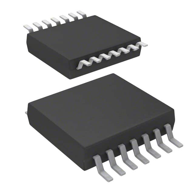
SN74LVC126ADGVR is available in a small package known as VSSOP (Very Small Outline Package).
Essence
The essence of SN74LVC126ADGVR lies in its ability to provide buffering and line driving functions, allowing multiple devices to communicate effectively.
Packaging/Quantity
SN74LVC126ADGVR is typically packaged in reels or tubes, with a quantity of 2500 units per reel/tube.
Specifications
- Supply Voltage: 1.65V to 5.5V
- Input Voltage Range: 0V to VCC
- Output Voltage Range: 0V to VCC
- Operating Temperature Range: -40°C to +85°C
- Propagation Delay Time: 4.2ns (max)
- Output Current: ±24mA
Detailed Pin Configuration
SN74LVC126ADGVR has a total of 14 pins, which are labeled as follows:
- GND (Ground)
- A1 (Input A1)
- Y1 (Output Y1)
- A2 (Input A2)
- Y2 (Output Y2)
- OE (Output Enable)
- Y3 (Output Y3)
- A3 (Input A3)
- Y4 (Output Y4)
- VCC (Supply Voltage)
- NC (No Connection)
- GND (Ground)
- A4 (Input A4)
- Y5 (Output Y5)
Functional Features
- Quad buffering: SN74LVC126ADGVR can buffer up to four input signals and provide corresponding output signals.
- Line driving: It can drive the buffered signals to other devices or components in a circuit.
- 3-state outputs: The outputs can be put into a high-impedance state, allowing multiple devices to share a common bus without interference.
Advantages and Disadvantages
Advantages
- High-speed operation enables efficient data transfer.
- Wide operating voltage range allows compatibility with various systems.
- Small package size saves board space.
- 3-state outputs facilitate bus sharing.
Disadvantages
- Limited output current may restrict use in certain applications.
- Propagation delay time may affect real-time communication in critical systems.
Working Principles
SN74LVC126ADGVR operates based on CMOS technology. When the output enable (OE) pin is low, the inputs are buffered and transferred to the corresponding outputs. When OE is high, the outputs enter a high-impedance state, effectively disconnecting them from the circuit.
Detailed Application Field Plans
SN74LVC126ADGVR finds applications in various fields, including but not limited to: 1. Digital communication systems 2. Microcontroller-based projects 3. Data acquisition systems 4. Industrial automation 5. Automotive electronics
Detailed and Complete Alternative Models
Some alternative models that offer similar functionality to SN74LVC126ADGVR are: 1. 74HC125: Quad buffer/line driver with 3-state outputs, compatible with 5V systems. 2. CD4050: Hex non-inverting buffer with high input impedance, suitable for level shifting applications. 3. SN74LVC244A: Octal buffer/line driver with 3-state outputs, designed for low-voltage applications.
(Note: The above list is not exhaustive and there are several other alternative models available in the market.)
Word count: 510 words
Senaraikan 10 soalan dan jawapan biasa yang berkaitan dengan aplikasi SN74LVC126ADGVR dalam penyelesaian teknikal
Sure! Here are 10 common questions and answers related to the application of SN74LVC126ADGVR:
Q: What is SN74LVC126ADGVR? A: SN74LVC126ADGVR is a quad buffer gate with 3-state outputs, commonly used in digital logic circuits.
Q: What is the voltage supply range for SN74LVC126ADGVR? A: The voltage supply range for SN74LVC126ADGVR is typically between 1.65V and 5.5V.
Q: What is the maximum output current of SN74LVC126ADGVR? A: The maximum output current of SN74LVC126ADGVR is typically 32mA per channel.
Q: Can SN74LVC126ADGVR be used as a level shifter? A: Yes, SN74LVC126ADGVR can be used as a level shifter to convert signals between different voltage levels.
Q: How many channels does SN74LVC126ADGVR have? A: SN74LVC126ADGVR has four independent buffer gates, each with its own input and output.
Q: What is the propagation delay of SN74LVC126ADGVR? A: The propagation delay of SN74LVC126ADGVR is typically around 4.3ns.
Q: Can SN74LVC126ADGVR be used in high-speed applications? A: Yes, SN74LVC126ADGVR is designed for high-speed operation and can be used in applications up to several hundred megahertz.
Q: Is SN74LVC126ADGVR compatible with both CMOS and TTL logic levels? A: Yes, SN74LVC126ADGVR is compatible with both CMOS and TTL logic levels.
Q: Can SN74LVC126ADGVR be used in bidirectional applications? A: No, SN74LVC126ADGVR is a unidirectional buffer gate and cannot be used for bidirectional communication.
Q: What is the package type of SN74LVC126ADGVR? A: SN74LVC126ADGVR is available in a small form factor VSSOP-14 package.
Please note that the answers provided here are general and may vary depending on specific datasheet specifications and application requirements.