

SN74LVC1G125YZAR
Product Overview
- Category: Integrated Circuit (IC)
- Use: Buffer/Driver
- Characteristics: Single Gate, Non-Inverting, 3-State Output
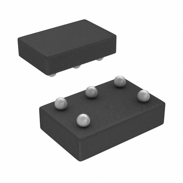
- Package: SOT-23-5
- Essence: Logic Level Shifter
- Packaging/Quantity: Tape and Reel, 3000 pieces per reel
Specifications
- Supply Voltage Range: 1.65V to 5.5V
- Input Voltage Range: 0V to VCC
- Output Voltage Range: 0V to VCC
- Maximum Operating Frequency: 400MHz
- Propagation Delay: 4.2ns (typical)
- Output Drive Capability: ±24mA
- Operating Temperature Range: -40°C to +85°C
Detailed Pin Configuration
The SN74LVC1G125YZAR has a total of 5 pins:
- GND (Ground): Connected to the ground reference of the circuit.
- OE (Output Enable): Controls the output state of the buffer.
- A (Input): Data input pin.
- Y (Output): Buffered output pin.
- VCC (Supply Voltage): Connected to the positive supply voltage.
Functional Features
- Single gate buffer with non-inverting 3-state output.
- Provides level shifting between different logic families.
- Allows bidirectional data flow when the output is disabled.
- Supports high-speed operation up to 400MHz.
- Low power consumption and wide operating voltage range.
Advantages and Disadvantages
Advantages: - Small package size allows for space-efficient designs. - Wide operating voltage range enables compatibility with various systems. - High-speed operation makes it suitable for time-critical applications. - 3-state output provides flexibility in controlling data flow.
Disadvantages: - Limited output drive capability may not be suitable for high-current applications. - Single gate design restricts the number of inputs and outputs.
Working Principles
The SN74LVC1G125YZAR is a logic level shifter that allows interfacing between different voltage domains. It operates by receiving a digital input signal (A) and buffering it to the output pin (Y). The output state can be controlled using the OE pin. When OE is low, the buffer is enabled, and the input signal is passed through to the output. When OE is high, the buffer is disabled, and the output enters a high-impedance state.
The device is powered by a supply voltage (VCC) within the specified range. It provides reliable logic level shifting while consuming minimal power. The small package size makes it suitable for space-constrained designs.
Detailed Application Field Plans
The SN74LVC1G125YZAR finds applications in various fields, including:
- Consumer Electronics: Used in smartphones, tablets, and portable devices for level shifting between different voltage domains.
- Industrial Automation: Enables communication between different logic families in control systems and sensors.
- Automotive Electronics: Facilitates data transfer between different components with varying voltage levels.
- Internet of Things (IoT): Allows integration of sensors and actuators operating at different voltage levels.
- Communication Systems: Used in networking equipment and data transmission interfaces for voltage level conversion.
Detailed and Complete Alternative Models
- SN74LVC1G07DBVR: Single Buffer/Driver with Open-Drain Output, SOT-23-5 package.
- SN74LVC1G34DCKR: Single Buffer/Driver with Schmitt-Trigger Input, SC-70-5 package.
- SN74LVC1G08DCKR: Single AND Gate, SC-70-5 package.
- SN74LVC1G14DBVR: Single Schmitt-Trigger Inverter, SOT-23-5 package.
- SN74LVC1G86DCKR: Single XOR Gate, SC-70-5 package.
These alternative models offer similar functionality and can be used as replacements for the SN74LVC1G125YZAR in various applications.
Word count: 491 words
Senaraikan 10 soalan dan jawapan biasa yang berkaitan dengan aplikasi SN74LVC1G125YZAR dalam penyelesaian teknikal
Sure! Here are 10 common questions and answers related to the application of SN74LVC1G125YZAR:
Q1: What is SN74LVC1G125YZAR? A1: SN74LVC1G125YZAR is a single bus buffer gate with 3-state output. It is commonly used in digital logic circuits for signal buffering and level shifting.
Q2: What is the operating voltage range of SN74LVC1G125YZAR? A2: The operating voltage range of SN74LVC1G125YZAR is from 1.65V to 5.5V.
Q3: What is the maximum output current of SN74LVC1G125YZAR? A3: The maximum output current of SN74LVC1G125YZAR is typically 32mA.
Q4: Can SN74LVC1G125YZAR be used as a level shifter? A4: Yes, SN74LVC1G125YZAR can be used as a level shifter to convert signals between different voltage levels.
Q5: What is the maximum propagation delay of SN74LVC1G125YZAR? A5: The maximum propagation delay of SN74LVC1G125YZAR is typically 4.3ns.
Q6: Can SN74LVC1G125YZAR drive capacitive loads? A6: Yes, SN74LVC1G125YZAR can drive capacitive loads up to a certain limit. However, it is recommended to refer to the datasheet for specific details.
Q7: Is SN74LVC1G125YZAR compatible with other logic families? A7: Yes, SN74LVC1G125YZAR is compatible with various logic families such as TTL, CMOS, and LVTTL.
Q8: Can SN74LVC1G125YZAR be used in high-speed applications? A8: Yes, SN74LVC1G125YZAR is suitable for high-speed applications due to its low propagation delay and fast switching characteristics.
Q9: What is the package type of SN74LVC1G125YZAR? A9: SN74LVC1G125YZAR is available in a small SOT-23-5 package.
Q10: Are there any specific precautions to consider when using SN74LVC1G125YZAR? A10: It is important to ensure that the power supply voltage does not exceed the specified range, and to follow the recommended operating conditions mentioned in the datasheet. Additionally, proper decoupling capacitors should be used to minimize noise and ensure stable operation.
Please note that these answers are general and it is always recommended to refer to the datasheet and consult with the manufacturer for specific application requirements.