

SN74LVC2G126YEPR
Product Overview
- Category: Integrated Circuit (IC)
- Use: Logic Gate Buffer/Driver
- Characteristics: Dual Bus Buffer Gate with 3-State Outputs
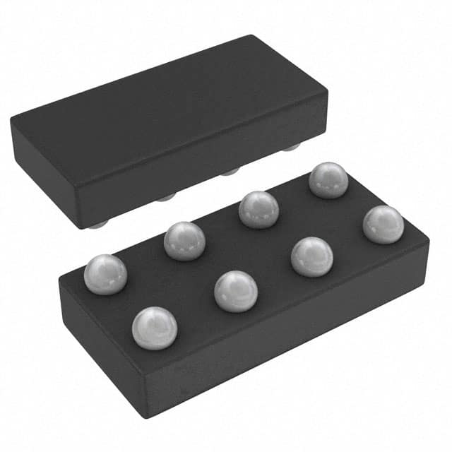
- Package: 8-pin VSSOP (Very Small Outline Package)
- Essence: Provides voltage level shifting and signal buffering capabilities
- Packaging/Quantity: Tape and Reel, 2500 units per reel
Specifications
- Supply Voltage Range: 1.65V to 5.5V
- High-Level Input Voltage: 2V to VCC + 0.5V
- Low-Level Input Voltage: -0.5V to 0.8V
- High-Level Output Voltage: VCC - 0.4V
- Low-Level Output Voltage: 0.4V
- Maximum Operating Frequency: 100MHz
- Propagation Delay Time: 4.6ns (typical)
Detailed Pin Configuration
The SN74LVC2G126YEPR has the following pin configuration:
___________
OE   -|           |- VCC
A    -|           |- B
Y    -|           |- GND
     -|           |- Y
GND  -|           |- A
B    -|           |- OE
VCC  -|           |- NC
     -|___________|-
Functional Features
- Dual bus buffer gate with 3-state outputs
- Supports voltage level shifting between different logic families
- Provides signal buffering to prevent signal degradation
- Allows bidirectional data flow
- Enables/disables output using the Output Enable (OE) pin
Advantages and Disadvantages
Advantages: - Wide supply voltage range allows compatibility with various systems - Fast propagation delay time ensures efficient signal transmission - Small package size saves board space - 3-state outputs provide flexibility in bus sharing applications
Disadvantages: - Limited maximum operating frequency compared to some other ICs - Not suitable for high-speed applications requiring very low propagation delay
Working Principles
The SN74LVC2G126YEPR is a dual bus buffer gate that operates by receiving input signals on the A and B pins. The logic level of these inputs determines the output state of the Y pin. When the OE pin is low, the outputs are enabled and mirror the inputs. Conversely, when the OE pin is high, the outputs are disabled and enter a high-impedance state.
The IC is designed to provide voltage level shifting between different logic families, allowing seamless integration of devices with varying voltage requirements. It also acts as a buffer, preventing signal degradation during transmission.
Detailed Application Field Plans
The SN74LVC2G126YEPR is commonly used in various digital systems and communication interfaces. Some specific application fields include:
- Microcontrollers: Provides level shifting and buffering capabilities for interfacing microcontrollers with different voltage levels.
- Communication Interfaces: Enables bidirectional data flow and voltage level translation between different communication protocols such as UART, SPI, and I2C.
- Industrial Automation: Used in control systems to interface sensors and actuators with different voltage requirements.
- Automotive Electronics: Facilitates signal buffering and level shifting in automotive electronic modules, such as body control units and infotainment systems.
Detailed and Complete Alternative Models
- SN74LVC2G07: Dual Buffer/Driver with Open-Drain Outputs
- SN74LVC2G34: Dual Buffer/Driver with Schmitt-Trigger Inputs
- SN74LVC2G241: Dual Buffer/Driver with 3-State Outputs and Series Resistor on Outputs
These alternative models offer similar functionality but may have different characteristics, package options, or additional features to suit specific application requirements.
Word count: 446 words
Senaraikan 10 soalan dan jawapan biasa yang berkaitan dengan aplikasi SN74LVC2G126YEPR dalam penyelesaian teknikal
Sure! Here are 10 common questions and answers related to the application of SN74LVC2G126YEPR:
Q: What is SN74LVC2G126YEPR? A: SN74LVC2G126YEPR is a dual bus buffer gate with 3-state outputs, commonly used in digital logic applications.
Q: What is the operating voltage range for SN74LVC2G126YEPR? A: The operating voltage range for SN74LVC2G126YEPR is typically between 1.65V and 5.5V.
Q: What is the maximum output current that SN74LVC2G126YEPR can drive? A: SN74LVC2G126YEPR can drive up to 32mA of output current per channel.
Q: Can SN74LVC2G126YEPR be used as a level shifter? A: Yes, SN74LVC2G126YEPR can be used as a level shifter to convert signals between different voltage levels.
Q: How many channels does SN74LVC2G126YEPR have? A: SN74LVC2G126YEPR has two independent channels.
Q: What is the propagation delay of SN74LVC2G126YEPR? A: The typical propagation delay of SN74LVC2G126YEPR is around 4.7ns.
Q: Can SN74LVC2G126YEPR be used in high-speed applications? A: Yes, SN74LVC2G126YEPR is designed for high-speed operation and can be used in applications with fast switching requirements.
Q: Does SN74LVC2G126YEPR have built-in ESD protection? A: Yes, SN74LVC2G126YEPR has built-in ESD protection to safeguard against electrostatic discharge.
Q: Can SN74LVC2G126YEPR be used in battery-powered applications? A: Yes, SN74LVC2G126YEPR has a wide operating voltage range and low power consumption, making it suitable for battery-powered applications.
Q: What is the package type of SN74LVC2G126YEPR? A: SN74LVC2G126YEPR is available in a small footprint 8-pin VSSOP package.
Please note that these answers are general and may vary depending on specific datasheet specifications and application requirements.