

SN74LVC2G240YEPR
Product Overview
- Category: Integrated Circuit (IC)
- Use: Logic Gate
- Characteristics: Dual Buffer/Driver, Non-Inverting, 3-State Output
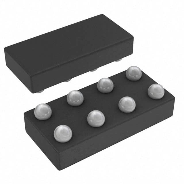
- Package: 8-pin VSSOP (Very Small Outline Package)
- Essence: High-speed CMOS technology for low power consumption and high noise immunity
- Packaging/Quantity: Tape and Reel, 2500 units per reel
Specifications
- Supply Voltage Range: 1.65V to 5.5V
- Input Voltage Range: -0.5V to VCC + 0.5V
- Output Voltage Range: 0V to VCC
- Maximum Operating Frequency: 100MHz
- Propagation Delay: 4.7ns (typical)
- Output Drive Capability: ±24mA
- Operating Temperature Range: -40°C to +85°C
Detailed Pin Configuration
The SN74LVC2G240YEPR has the following pin configuration:
___________
   A1 |           | VCC
   A2 |           | B1
   GND |           | B2
   OE  |           | Y1
   Y2  |           | GND
       -------------
Functional Features
- Dual Buffer/Driver: Provides two independent buffer/driver circuits in a single package.
- Non-Inverting: The input signal is reproduced at the output without any inversion.
- 3-State Output: Allows the output to be in a high-impedance state, enabling multiple devices to share a common bus.
Advantages and Disadvantages
Advantages: - High-speed operation: Suitable for applications requiring fast switching speeds. - Low power consumption: Helps conserve energy in battery-powered devices. - High noise immunity: Resistant to external noise interference. - Small package size: Saves board space in compact designs.
Disadvantages: - Limited output drive capability: May not be suitable for driving heavy loads. - Narrow supply voltage range: Requires a regulated power supply within the specified range.
Working Principles
The SN74LVC2G240YEPR is based on high-speed CMOS technology. It operates by receiving input signals (A1, A2) and reproducing them at the outputs (Y1, Y2) without any inversion. The OE pin controls the output state, allowing it to be either active or in a high-impedance state.
Detailed Application Field Plans
The SN74LVC2G240YEPR is commonly used in various applications, including:
- Communication Systems: Used for signal buffering and level shifting in data transmission circuits.
- Industrial Automation: Enables interfacing between different logic levels in control systems.
- Consumer Electronics: Utilized in portable devices, such as smartphones and tablets, for signal amplification and level conversion.
- Automotive Electronics: Suitable for automotive control units, providing reliable signal conditioning and driving capabilities.
- IoT (Internet of Things): Used in sensor nodes and edge devices for signal processing and interfacing with microcontrollers.
Detailed and Complete Alternative Models
- SN74LVC2G07: Dual Buffer/Driver with Open-Drain Outputs
- SN74LVC2G17: Dual Schmitt-Trigger Buffer/Driver
- SN74LVC2G34: Dual Buffer/Driver with 3-State Outputs
- SN74LVC2G125: Dual Bus Buffer/Driver with 3-State Outputs
- SN74LVC2G241: Dual Buffer/Driver with Inverting Outputs
These alternative models offer similar functionality and can be considered as replacements for the SN74LVC2G240YEPR in different applications.
Word count: 490 words
Senaraikan 10 soalan dan jawapan biasa yang berkaitan dengan aplikasi SN74LVC2G240YEPR dalam penyelesaian teknikal
Sure! Here are 10 common questions and answers related to the application of SN74LVC2G240YEPR:
Q: What is SN74LVC2G240YEPR? A: SN74LVC2G240YEPR is a dual buffer/line driver IC (integrated circuit) designed for voltage level translation applications.
Q: What is the operating voltage range of SN74LVC2G240YEPR? A: The operating voltage range is from 1.65V to 5.5V.
Q: What is the maximum output current of SN74LVC2G240YEPR? A: The maximum output current is typically 24mA.
Q: Can SN74LVC2G240YEPR be used for bidirectional level translation? A: Yes, it can be used for bidirectional level translation as it has separate input and output voltage pins.
Q: What is the maximum propagation delay of SN74LVC2G240YEPR? A: The maximum propagation delay is typically 4.3ns.
Q: Is SN74LVC2G240YEPR compatible with both CMOS and TTL logic levels? A: Yes, it is compatible with both CMOS and TTL logic levels.
Q: Can SN74LVC2G240YEPR be used in high-speed applications? A: Yes, it is suitable for high-speed applications due to its low propagation delay and high-speed operation.
Q: Does SN74LVC2G240YEPR have built-in ESD protection? A: Yes, it has built-in ESD (Electrostatic Discharge) protection to prevent damage from static electricity.
Q: Can SN74LVC2G240YEPR be used in battery-powered applications? A: Yes, it can be used in battery-powered applications as it operates at low voltage levels.
Q: What is the package type of SN74LVC2G240YEPR? A: SN74LVC2G240YEPR is available in a small SOT-23-8 package.
Please note that these answers are general and may vary depending on the specific datasheet and application requirements.