

SN74LVC3G06YEPR
Product Overview
- Category: Integrated Circuit
- Use: Logic Gate
- Characteristics: Triple Inverter Buffer/Driver
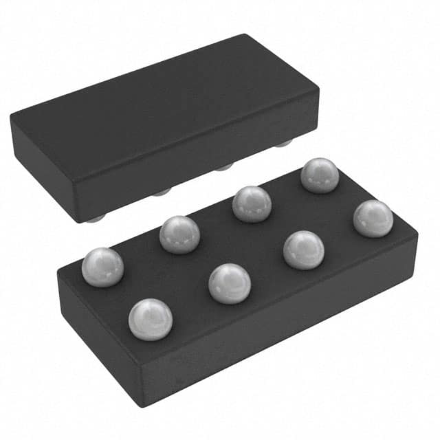
- Package: 8-pin VSSOP
- Essence: High-speed CMOS technology
- Packaging/Quantity: Tape and Reel, 2500 units per reel
Specifications
- Supply Voltage Range: 1.65V to 5.5V
- Input Voltage Range: -0.5V to VCC + 0.5V
- Output Voltage Range: 0V to VCC
- Maximum Operating Frequency: 100MHz
- Propagation Delay: 4.2ns (typical)
- Low Power Consumption: 10µA (maximum)
Detailed Pin Configuration
The SN74LVC3G06YEPR has the following pin configuration:
___________
   1 |             | 8
   2 |             | 7
   3 |             | 6
   4 |             | 5
      ¯¯¯¯¯¯¯¯¯¯¯¯
Pin Description: 1. Input A 2. Output Y 3. Input B 4. GND 5. Output Y 6. Input C 7. VCC 8. NC (No Connection)
Functional Features
- Triple inverter buffer/driver with open-drain outputs
- Provides voltage level shifting and signal amplification
- Supports bidirectional communication
- High-speed operation suitable for various applications
- Low power consumption for energy-efficient designs
- Wide supply voltage range allows compatibility with different systems
Advantages and Disadvantages
Advantages: - High-speed CMOS technology ensures fast and reliable operation - Triple inverter design provides robust signal buffering capabilities - Open-drain outputs allow flexible interfacing with other devices - Wide supply voltage range enhances compatibility with different systems
Disadvantages: - Limited number of inputs and outputs restricts the complexity of circuits that can be implemented - Open-drain outputs require external pull-up resistors for proper signal level restoration
Working Principles
The SN74LVC3G06YEPR is a triple inverter buffer/driver integrated circuit. It utilizes high-speed CMOS technology to provide fast and reliable logic level shifting and signal amplification. The open-drain outputs allow bidirectional communication and flexible interfacing with other devices.
When an input signal is applied to one of the three input pins (A, B, or C), the corresponding output pin (Y) will invert the signal and drive it onto the connected circuit. The open-drain configuration requires an external pull-up resistor to restore the output signal to the desired logic level.
The wide supply voltage range allows the SN74LVC3G06YEPR to be used in various applications, including battery-powered devices and industrial control systems. Its low power consumption makes it suitable for energy-efficient designs.
Detailed Application Field Plans
The SN74LVC3G06YEPR can be used in a wide range of applications, including:
- Communication Systems: The open-drain outputs make it ideal for bidirectional communication interfaces, such as I2C and SMBus.
- Sensor Interfacing: The voltage level shifting capability enables seamless integration of sensors with different logic voltage levels.
- Industrial Control Systems: The high-speed operation and wide supply voltage range make it suitable for controlling various industrial processes.
- Battery-Powered Devices: The low power consumption ensures extended battery life in portable electronics.
- Automotive Electronics: The robust design and wide temperature range make it suitable for automotive applications, such as engine control units and infotainment systems.
Detailed and Complete Alternative Models
- SN74LVC3G07: Triple Buffer/Driver with Open-Drain Outputs
- SN74LVC3G08: Triple AND Gate with Open-Drain Outputs
- SN74LVC3G14: Triple Schmitt-Trigger Inverter with Open-Drain Outputs
- SN74LVC3G17: Triple Schmitt-Trigger Buffer/Driver with Open-Drain Outputs
- SN74LVC3G34: Triple Buffer/Driver with 5V Tolerant Inputs and Open-Drain Outputs
These alternative models offer similar functionality and can be used as replacements for the SN74LVC3G06YEPR in various applications.
Word count: 530 words
Senaraikan 10 soalan dan jawapan biasa yang berkaitan dengan aplikasi SN74LVC3G06YEPR dalam penyelesaian teknikal
Sure! Here are 10 common questions and answers related to the application of SN74LVC3G06YEPR:
Q: What is SN74LVC3G06YEPR? A: SN74LVC3G06YEPR is a triple inverter gate IC (integrated circuit) that is commonly used in digital logic applications.
Q: What is the voltage supply range for SN74LVC3G06YEPR? A: The voltage supply range for SN74LVC3G06YEPR is typically between 1.65V and 5.5V.
Q: What is the maximum output current of SN74LVC3G06YEPR? A: The maximum output current of SN74LVC3G06YEPR is typically around 32mA.
Q: Can SN74LVC3G06YEPR be used as a level shifter? A: Yes, SN74LVC3G06YEPR can be used as a level shifter to convert signals between different voltage levels.
Q: What is the propagation delay of SN74LVC3G06YEPR? A: The propagation delay of SN74LVC3G06YEPR is typically around 3.7ns.
Q: Is SN74LVC3G06YEPR suitable for high-speed applications? A: Yes, SN74LVC3G06YEPR is designed for high-speed operation and can be used in various high-frequency applications.
Q: Can SN74LVC3G06YEPR drive capacitive loads? A: Yes, SN74LVC3G06YEPR has a good ability to drive capacitive loads, making it suitable for driving long traces or cables.
Q: What is the temperature range for SN74LVC3G06YEPR? A: The temperature range for SN74LVC3G06YEPR is typically between -40°C and 85°C.
Q: Can SN74LVC3G06YEPR be used in battery-powered applications? A: Yes, SN74LVC3G06YEPR has a low power consumption and can be used in battery-powered devices.
Q: Are there any alternative ICs to SN74LVC3G06YEPR? A: Yes, there are alternative ICs available from different manufacturers, such as 74LVC3G06 or NC7SZ06, which serve similar functions.
Please note that the answers provided here are general and may vary depending on specific datasheet specifications and application requirements.