

SN74LVCC3245ADBRG4
Product Overview
- Category: Integrated Circuit (IC)
- Use: Level Shifter and Bus Transceiver
- Characteristics: Bi-directional voltage level translation, 3-state outputs, low power consumption
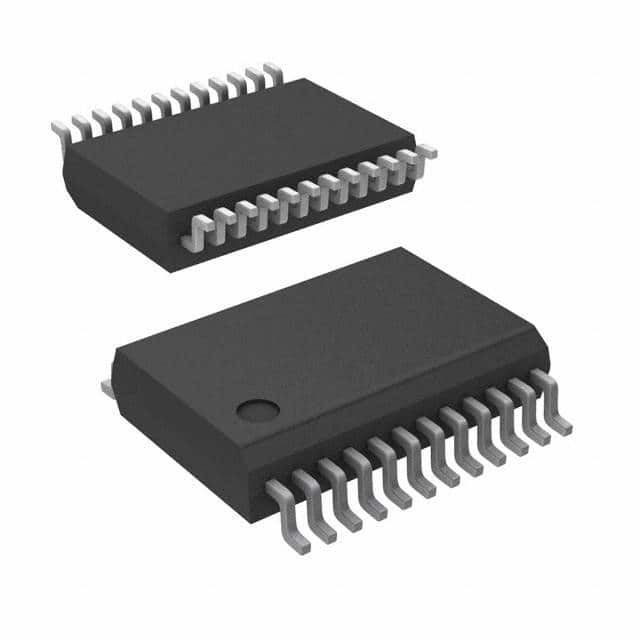
- Package: SSOP-20
- Essence: A high-performance level shifter and bus transceiver IC designed for voltage level translation between different logic families.
- Packaging/Quantity: Tape and Reel, 2500 units per reel
Specifications
- Supply Voltage Range: 1.65V to 5.5V
- Logic Family: LVCC
- Number of Channels: 8
- Input/Output Compatibility: TTL, CMOS
- Output Drive Capability: ±24mA
- Propagation Delay: 6ns (typical)
- Operating Temperature Range: -40°C to +85°C
Detailed Pin Configuration
The SN74LVCC3245ADBRG4 has a total of 20 pins arranged as follows:
+-------------------+
    OE1 --|1                20|-- VCC
   DIR1 --|2                19|-- GND
   B1Ax --|3                18|-- B1Bx
   B1Bx --|4                17|-- A1Bx
   A1Bx --|5     SN74LVCC    16|-- A1Ax
   A1Ax --|6     3245A       15|-- B1Ax
   B1Ax --|7     DBRG4       14|-- DIR2
   DIR2 --|8                13|-- OE2
   OE2 -- |9                12|-- B2Bx
  B2Bx -- |10               11|-- A2Bx
          +-------------------+
Functional Features
- Bi-directional voltage level translation between TTL and CMOS logic families.
- 3-state outputs allow multiple devices to share a common bus.
- Low power consumption for energy-efficient operation.
- High-speed operation with low propagation delay.
Advantages and Disadvantages
Advantages: - Wide supply voltage range allows compatibility with various systems. - Supports bidirectional communication between different logic families. - 3-state outputs enable efficient bus sharing.
Disadvantages: - Limited number of channels (8) may not be suitable for applications requiring a higher channel count. - Propagation delay may affect timing-sensitive applications.
Working Principles
The SN74LVCC3245ADBRG4 is designed to facilitate voltage level translation between different logic families, specifically TTL and CMOS. It utilizes a combination of input/output buffers and control circuitry to achieve bidirectional communication. The direction of data flow is controlled by the DIR1 and DIR2 pins, while the OE1 and OE2 pins enable/disable the output drivers. The IC operates within a specified supply voltage range and provides 3-state outputs, allowing multiple devices to share a common bus.
Detailed Application Field Plans
The SN74LVCC3245ADBRG4 finds application in various fields where voltage level translation is required between TTL and CMOS logic families. Some potential application areas include:
- Microcontroller interfacing: The IC can be used to interface microcontrollers operating at different voltage levels, enabling seamless communication between them.
- Communication systems: It can be employed in communication systems to translate voltage levels between different modules or subsystems.
- Industrial automation: The IC can facilitate voltage level translation in industrial automation systems, ensuring compatibility between different components.
- Consumer electronics: It can be utilized in consumer electronic devices to enable communication between different logic families, such as between microcontrollers and display modules.
Detailed and Complete Alternative Models
- SN74LVC4245APWR: Similar to SN74LVCC3245ADBRG4, but operates at a lower supply voltage range (1.65V to 3.6V).
- SN74HCT245N: A non-inverting octal bus transceiver IC compatible with TTL logic family.
- CD4504BE: Hex voltage level shifter IC designed for CMOS to TTL translation.
These alternative models offer similar functionality and can be considered as substitutes based on specific application requirements.
Word count: 529 words
Senaraikan 10 soalan dan jawapan biasa yang berkaitan dengan aplikasi SN74LVCC3245ADBRG4 dalam penyelesaian teknikal
Sure! Here are 10 common questions and answers related to the application of SN74LVCC3245ADBRG4:
Q: What is SN74LVCC3245ADBRG4? A: SN74LVCC3245ADBRG4 is a bidirectional voltage level translator and voltage-level shifter integrated circuit (IC) commonly used in technical solutions.
Q: What is the operating voltage range of SN74LVCC3245ADBRG4? A: SN74LVCC3245ADBRG4 operates within a voltage range of 1.65V to 5.5V.
Q: What is the maximum data transfer rate supported by SN74LVCC3245ADBRG4? A: SN74LVCC3245ADBRG4 supports a maximum data transfer rate of 100 Mbps.
Q: Can SN74LVCC3245ADBRG4 be used for level shifting between different voltage domains? A: Yes, SN74LVCC3245ADBRG4 is designed specifically for voltage level translation and can be used for level shifting between different voltage domains.
Q: How many bidirectional channels does SN74LVCC3245ADBRG4 have? A: SN74LVCC3245ADBRG4 has 8 bidirectional channels.
Q: What is the typical propagation delay of SN74LVCC3245ADBRG4? A: The typical propagation delay of SN74LVCC3245ADBRG4 is around 5 ns.
Q: Can SN74LVCC3245ADBRG4 be used with both CMOS and TTL logic levels? A: Yes, SN74LVCC3245ADBRG4 is compatible with both CMOS and TTL logic levels.
Q: What is the maximum output current that SN74LVCC3245ADBRG4 can drive? A: SN74LVCC3245ADBRG4 can drive a maximum output current of 24 mA.
Q: Can SN74LVCC3245ADBRG4 be used in bi-directional data buses? A: Yes, SN74LVCC3245ADBRG4 is commonly used in bi-directional data buses to enable communication between different voltage domains.
Q: Is SN74LVCC3245ADBRG4 available in different package options? A: Yes, SN74LVCC3245ADBRG4 is available in various package options, such as SSOP, TSSOP, and VQFN, to suit different application requirements.
Please note that these answers are general and may vary depending on specific datasheet specifications and application requirements.