

TPS61050DRCR
Product Overview
Category
The TPS61050DRCR belongs to the category of integrated circuits (ICs) and specifically falls under the voltage regulators - switching regulators classification.
Use
This product is primarily used as a boost converter, which means it increases the input voltage to a higher output voltage level. It is commonly employed in various electronic devices where a stable and regulated power supply is required.
Characteristics
- High efficiency: The TPS61050DRCR offers high conversion efficiency, ensuring minimal power loss during voltage conversion.
- Wide input voltage range: It can accept input voltages ranging from 1.8V to 6V, making it suitable for a wide range of applications.
- Adjustable output voltage: The output voltage can be adjusted using external resistors, providing flexibility in meeting specific requirements.
- Low quiescent current: The device has a low quiescent current, resulting in reduced power consumption during standby or idle modes.
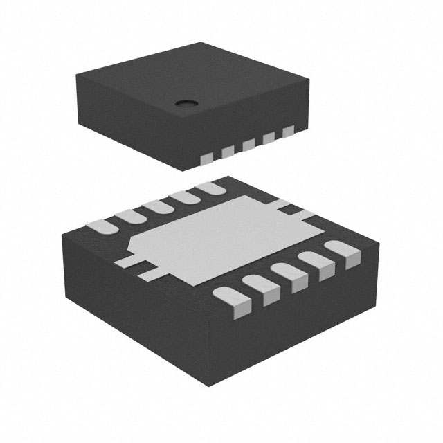
Package
The TPS61050DRCR comes in a small outline package (SOT-23-6), which is a surface-mount package with six pins. This package type ensures easy integration onto circuit boards and facilitates efficient heat dissipation.
Essence
The essence of the TPS61050DRCR lies in its ability to efficiently step up input voltages to higher levels, enabling reliable power supply solutions in various electronic applications.
Packaging/Quantity
The TPS61050DRCR is typically available in tape and reel packaging, with a quantity of 3000 units per reel. This packaging format ensures ease of handling during manufacturing processes and provides protection against physical damage.
Specifications
- Input Voltage Range: 1.8V to 6V
- Output Voltage Range: Adjustable (based on external resistors)
- Switching Frequency: Up to 1.2MHz
- Quiescent Current: 40µA (typical)
- Operating Temperature Range: -40°C to +85°C
- Efficiency: Up to 90%
Detailed Pin Configuration
The TPS61050DRCR has six pins arranged as follows:
```
| | --| VIN SW |-- --| GND FB |-- --| EN VOUT|-- |___________| ```
- VIN: Input voltage pin.
- SW: Switching node pin.
- GND: Ground reference pin.
- FB: Feedback pin for output voltage regulation.
- EN: Enable pin for turning the device on/off.
- VOUT: Output voltage pin.
Functional Features
- Wide input voltage range: The TPS61050DRCR can accept a broad range of input voltages, making it suitable for various power supply applications.
- Adjustable output voltage: The output voltage can be easily adjusted using external resistors, allowing customization based on specific requirements.
- High efficiency: With its high conversion efficiency, the device minimizes power loss during voltage conversion, resulting in improved overall system efficiency.
- Low quiescent current: The low quiescent current ensures reduced power consumption during standby or idle modes, enhancing energy efficiency.
Advantages and Disadvantages
Advantages
- High efficiency leads to reduced power dissipation.
- Wide input voltage range enables versatile application possibilities.
- Adjustable output voltage allows flexibility in meeting specific requirements.
- Low quiescent current enhances energy efficiency during idle periods.
Disadvantages
- Limited maximum output current capability.
- Requires external components for proper operation.
- Sensitive to excessive heat, necessitating appropriate thermal management.
Working Principles
The TPS61050DRCR operates as a boost converter, utilizing a switching regulator topology. It employs an internal power MOSFET switch to control the energy transfer from the input to the output. The device operates in a pulse-width modulation (PWM) mode, where the duty cycle of the switch is adjusted to regulate the output voltage.
When the input voltage is applied, the internal switch rapidly turns on and off, creating a square wave voltage at the switching node. This square wave is then filtered and stepped up to the desired output voltage level using an inductor and capacitor combination. The feedback pin monitors the output voltage and adjusts the duty cycle accordingly to maintain a stable output.
Detailed Application Field Plans
The TPS61050DRCR finds applications in various electronic devices and systems, including but not limited to: - Battery-powered portable devices - Wireless communication systems - LED backlighting for displays - Industrial automation equipment - Automotive electronics - Medical devices
Detailed and Complete Alternative Models
Some alternative models that offer similar functionality to the TPS61050DRCR include: - TPS61051DRCR - TPS61052DRCR - T
Senaraikan 10 soalan dan jawapan biasa yang berkaitan dengan aplikasi TPS61050DRCR dalam penyelesaian teknikal
Sure! Here are 10 common questions and answers related to the application of TPS61050DRCR in technical solutions:
Q: What is the TPS61050DRCR? A: The TPS61050DRCR is a boost converter integrated circuit (IC) that provides a regulated output voltage from a lower input voltage.
Q: What is the input voltage range for the TPS61050DRCR? A: The TPS61050DRCR has an input voltage range of 0.7V to 5.5V.
Q: What is the typical output voltage range of the TPS61050DRCR? A: The TPS61050DRCR can provide a regulated output voltage ranging from 1.8V to 5.5V.
Q: What is the maximum output current capability of the TPS61050DRCR? A: The TPS61050DRCR can deliver a maximum output current of 500mA.
Q: Can the TPS61050DRCR operate with a single lithium-ion battery as the input source? A: Yes, the TPS61050DRCR can efficiently boost the voltage from a single lithium-ion battery to power various applications.
Q: Does the TPS61050DRCR have built-in protection features? A: Yes, the TPS61050DRCR includes over-temperature protection, over-current protection, and under-voltage lockout to ensure safe operation.
Q: Can the TPS61050DRCR be used in portable electronic devices? A: Absolutely! The TPS61050DRCR is commonly used in portable electronic devices such as smartphones, tablets, and wearables.
Q: What is the efficiency of the TPS61050DRCR? A: The TPS61050DRCR has a high efficiency, typically above 90%, which helps to maximize battery life in portable applications.
Q: Can the TPS61050DRCR be used in automotive applications? A: Yes, the TPS61050DRCR is suitable for automotive applications that require voltage boosting, such as LED lighting or sensor systems.
Q: Are there any application notes or reference designs available for the TPS61050DRCR? A: Yes, Texas Instruments provides application notes and reference designs that can help engineers implement the TPS61050DRCR effectively in their designs.
Please note that these answers are general and may vary depending on specific design requirements and conditions. It's always recommended to refer to the datasheet and consult with the manufacturer for detailed information.