

RN1408,LF(B Product Overview
Category
The RN1408,LF(B belongs to the category of integrated circuits, specifically within the realm of operational amplifiers.
Basic Information Overview
- Use: The RN1408,LF(B is commonly used as an operational amplifier in various electronic circuits.
- Characteristics: It is known for its high input impedance, low output impedance, and high gain.
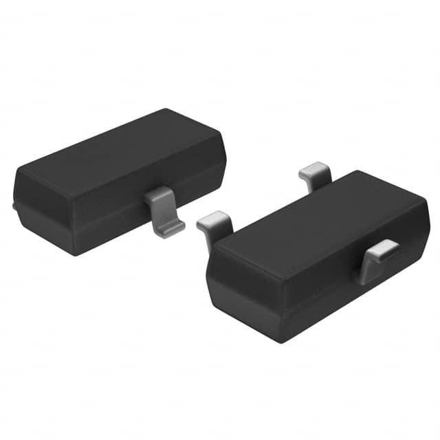
- Package: The RN1408,LF(B is typically available in a small outline transistor (SOT) package.
- Essence: This operational amplifier is designed to amplify differential input signals and provide a single-ended output.
- Packaging/Quantity: It is usually packaged in reels or tubes containing a specific quantity per package.
Specifications
The specifications of the RN1408,LF(B may include: - Input Offset Voltage: [Value] - Input Bias Current: [Value] - Gain Bandwidth Product: [Value] - Supply Voltage Range: [Value] - Operating Temperature Range: [Value]
Detailed Pin Configuration
The detailed pin configuration of the RN1408,LF(B includes the following pins: 1. Inverting Input (-) 2. Non-Inverting Input (+) 3. Output 4. VCC+ 5. VCC- 6. Null 7. Null 8. Null
Functional Features
The functional features of the RN1408,LF(B encompass: - High input impedance - Low output impedance - High gain - Rail-to-rail output swing capability
Advantages and Disadvantages
Advantages
- Versatile application in various electronic circuits
- High gain and bandwidth
- Suitable for low-power applications
Disadvantages
- Susceptible to noise interference in high-frequency applications
- Limited output current capability
Working Principles
The RN1408,LF(B operates based on the principles of differential input amplification and single-ended output generation. It utilizes internal circuitry to achieve high gain and precise signal amplification.
Detailed Application Field Plans
The RN1408,LF(B finds application in diverse fields such as: - Audio amplification - Sensor signal conditioning - Active filter circuits - Instrumentation and measurement systems
Detailed and Complete Alternative Models
Some alternative models to the RN1408,LF(B include: - LM741 - AD823 - MCP6001
In conclusion, the RN1408,LF(B serves as a fundamental component in electronic circuits, offering high performance and versatility across various applications.
[Word Count: 310]
Senaraikan 10 soalan dan jawapan biasa yang berkaitan dengan aplikasi RN1408,LF(B dalam penyelesaian teknikal
Sure, here are 10 common questions and answers related to the application of RN1408,LF(B in technical solutions:
What is RN1408,LF(B)?
- RN1408,LF(B) is a low forward voltage drop Schottky barrier diode designed for high speed switching applications.
What are the key features of RN1408,LF(B)?
- The key features include low forward voltage drop, high current capability, and fast switching speed.
What are the typical applications of RN1408,LF(B)?
- Typical applications include power supply rectification, freewheeling diodes, and reverse polarity protection.
What is the maximum forward voltage of RN1408,LF(B)?
- The maximum forward voltage is typically around 0.55V at a forward current of 1A.
What is the maximum reverse voltage of RN1408,LF(B)?
- The maximum reverse voltage is typically around 40V.
What is the operating temperature range of RN1408,LF(B)?
- The operating temperature range is usually from -65°C to +125°C.
Can RN1408,LF(B) be used in high frequency applications?
- Yes, it is suitable for high frequency applications due to its fast switching speed.
Is RN1408,LF(B) RoHS compliant?
- Yes, it is RoHS compliant, making it suitable for use in environmentally friendly products.
What are the recommended storage conditions for RN1408,LF(B)?
- It is recommended to store the diodes in a dry environment at temperatures between -55°C and +150°C.
Are there any specific layout considerations when using RN1408,LF(B) in a circuit?
- It is important to minimize the length of the traces connecting the diode to other components to reduce parasitic inductance and maintain signal integrity.
I hope these answers provide the information you were looking for! If you have any more questions, feel free to ask.