

TC7WPB8306L8X,LF
Basic Information Overview
- Category: Integrated Circuit (IC)
- Use: Logic Gate
- Characteristics:
- Low-power consumption
- High-speed operation
- Wide operating voltage range
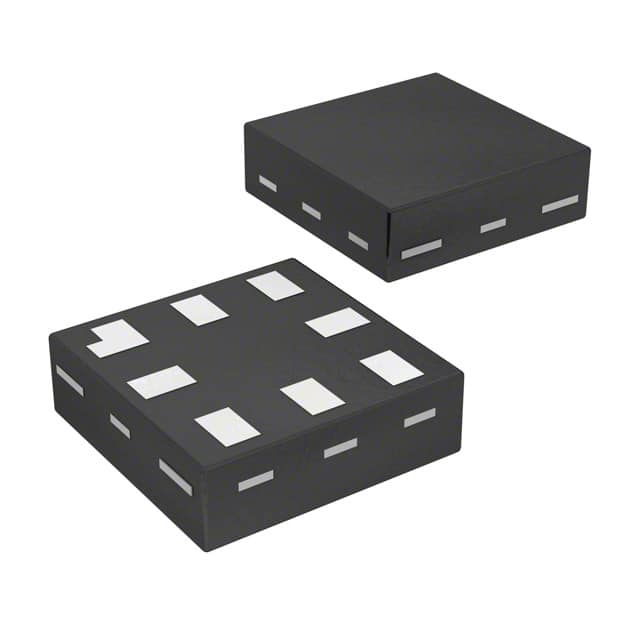
- Package: SOT-353 (5-pin package)
- Essence: N-channel MOSFET logic gate
- Packaging/Quantity: Tape and Reel, 3000 units per reel
Specifications
- Supply Voltage Range: 1.65V to 5.5V
- Input Voltage Range: 0V to VDD
- Output Voltage Range: 0V to VDD
- Operating Temperature Range: -40°C to +85°C
- Propagation Delay Time: 2.5ns (typical)
- Input Capacitance: 3pF (typical)
- Output Capacitance: 4pF (typical)
Detailed Pin Configuration
The TC7WPB8306L8X,LF has the following pin configuration:
```
| | --|1 5|-- --|2 4|-- |____| GND ```
Pin Description: 1. A: Input A 2. B: Input B 3. NC: No Connection 4. Y: Output 5. VDD: Power Supply
Functional Features
- Performs logical AND function on inputs A and B
- Provides a high-level output when both inputs are high
- Supports a wide range of supply voltages
- Low power consumption makes it suitable for battery-powered devices
- High-speed operation enables efficient data processing
Advantages
- Low power consumption extends battery life in portable devices
- High-speed operation allows for quick data processing
- Wide operating voltage range provides flexibility in various applications
- Small package size saves board space
- Reliable performance in a wide temperature range
Disadvantages
- Limited number of inputs (only two)
- Output is active high, which may not be suitable for all applications
- Not suitable for high-current applications due to its small package size
Working Principles
The TC7WPB8306L8X,LF is an N-channel MOSFET logic gate that performs the logical AND function. It consists of two input transistors and one output transistor. When both input A and input B are high, the output Y is driven to a high level. Otherwise, the output remains low.
Detailed Application Field Plans
The TC7WPB8306L8X,LF can be used in various applications, including: 1. Digital signal processing systems 2. Microcontrollers and microprocessors 3. Communication devices 4. Battery-powered devices 5. Industrial automation systems
Detailed and Complete Alternative Models
Some alternative models that can be considered as replacements for the TC7WPB8306L8X,LF include: 1. SN74LVC1G08DBVR - Single 2-Input Positive-AND Gate 2. CD4081BE - Quad 2-Input AND Gate 3. MC14081BCP - Quad 2-Input AND Gate 4. 74HC08N - Quad 2-Input AND Gate
These alternative models offer similar functionality and can be used as substitutes based on specific requirements.
Word count: 346 words
Senaraikan 10 soalan dan jawapan biasa yang berkaitan dengan aplikasi TC7WPB8306L8X,LF dalam penyelesaian teknikal
Sure! Here are 10 common questions and answers related to the application of TC7WPB8306L8X,LF in technical solutions:
1. What is TC7WPB8306L8X,LF? - TC7WPB8306L8X,LF is a specific model of a logic gate IC (integrated circuit) manufactured by Toshiba.
2. What is the function of TC7WPB8306L8X,LF? - TC7WPB8306L8X,LF is a triple 2-input AND gate that performs logical AND operations on two input signals.
3. What voltage levels does TC7WPB8306L8X,LF support? - TC7WPB8306L8X,LF supports a wide range of voltage levels, typically from 2V to 5.5V.
4. Can TC7WPB8306L8X,LF be used in both digital and analog circuits? - No, TC7WPB8306L8X,LF is specifically designed for digital circuits and is not suitable for analog applications.
5. What is the maximum operating frequency of TC7WPB8306L8X,LF? - The maximum operating frequency of TC7WPB8306L8X,LF is typically around 100 MHz.
6. How many gates are there in TC7WPB8306L8X,LF? - TC7WPB8306L8X,LF consists of three independent AND gates in a single package.
7. Can TC7WPB8306L8X,LF be used in high-speed applications? - Yes, TC7WPB8306L8X,LF is suitable for high-speed applications due to its fast propagation delay and transition times.
8. What is the power supply requirement for TC7WPB8306L8X,LF? - TC7WPB8306L8X,LF requires a power supply voltage between 2V and 5.5V.
9. Is TC7WPB8306L8X,LF compatible with other logic families? - Yes, TC7WPB8306L8X,LF is compatible with various logic families such as TTL (Transistor-Transistor Logic) and CMOS (Complementary Metal-Oxide-Semiconductor).
10. Can TC7WPB8306L8X,LF be used in battery-powered devices? - Yes, TC7WPB8306L8X,LF can be used in battery-powered devices as it operates within a wide range of voltage levels and has low power consumption.
Please note that the answers provided here are general and may vary depending on specific application requirements.