

XC2C256-6PQG208C
Product Overview
Category
XC2C256-6PQG208C belongs to the category of programmable logic devices (PLDs).
Use
This product is primarily used in digital circuit design and implementation. It provides a flexible and customizable solution for various applications.
Characteristics
- Programmable: The XC2C256-6PQG208C can be programmed to perform specific functions according to the user's requirements.
- High-density: With 256 macrocells, this PLD offers a high level of integration.
- Low power consumption: The device is designed to operate efficiently with minimal power consumption.
- Fast operation: The XC2C256-6PQG208C delivers high-speed performance, enabling rapid data processing.
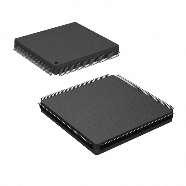
Package
The XC2C256-6PQG208C is available in a PQG208 package. This package type ensures easy installation and compatibility with standard PCB designs.
Essence
The essence of XC2C256-6PQG208C lies in its ability to provide reconfigurable logic functionality, allowing users to implement complex digital circuits without the need for custom hardware.
Packaging/Quantity
The XC2C256-6PQG208C is typically packaged individually and is available in various quantities depending on the customer's needs.
Specifications
- Logic Cells: 256
- I/O Pins: 208
- Operating Voltage: 3.3V
- Speed Grade: -6
- Maximum Frequency: 200 MHz
- Configuration Memory: Flash-based
Detailed Pin Configuration
The XC2C256-6PQG208C has a total of 208 I/O pins. These pins are distributed across the device and can be configured as inputs or outputs based on the user's requirements. The pin configuration diagram provides a detailed layout of the pins and their corresponding functions.
Functional Features
- Reconfigurable Logic: The XC2C256-6PQG208C allows users to modify the logic functionality of the device, enabling the implementation of different digital circuits.
- Flexible I/O Configuration: The device offers a wide range of I/O options, allowing for versatile connectivity with external components.
- On-Chip Memory: The XC2C256-6PQG208C includes flash-based configuration memory, which enables easy reprogramming of the device without the need for external storage.
Advantages and Disadvantages
Advantages
- Flexibility: The XC2C256-6PQG208C provides a flexible solution for digital circuit design, eliminating the need for custom hardware.
- High Integration: With 256 macrocells, this PLD offers a high level of integration, reducing the overall system complexity.
- Low Power Consumption: The device is designed to operate efficiently with minimal power consumption, making it suitable for battery-powered applications.
Disadvantages
- Learning Curve: Utilizing programmable logic devices requires knowledge of hardware description languages and digital circuit design principles.
- Limited Resources: While the XC2C256-6PQG208C offers a high level of integration, it may not be suitable for extremely complex designs that require more resources.
Working Principles
The XC2C256-6PQG208C operates based on the principle of reconfigurable logic. It consists of an array of configurable logic blocks (CLBs) interconnected through programmable interconnects. These CLBs can be programmed to implement various logic functions, allowing for the creation of complex digital circuits.
Detailed Application Field Plans
The XC2C256-6PQG208C finds applications in various fields, including:
- Industrial Automation: The device can be used to implement control systems for industrial processes, enabling efficient automation and monitoring.
- Communication Systems: XC2C256-6PQG208C can be utilized in the design of communication protocols and signal processing algorithms.
- Consumer Electronics: This PLD is suitable for applications such as gaming consoles, multimedia devices, and home automation systems.
- Automotive Electronics: The XC2C256-6PQG208C can be employed in automotive control systems, including engine management, safety features, and infotainment systems.
Detailed and Complete Alternative Models
- XC2C128-7VQG100C: A similar PLD with 128 macrocells and 100 I/O pins, offering a lower level of integration but at a reduced cost.
- XC2C384-10PQG208C: A higher-end model with 384 macrocells and 208 I/O pins, providing increased capacity for more complex designs.
- XC2C512-10FTG256C: A larger variant with 512 macrocells and 256 I/O pins, suitable for applications requiring extensive logic resources.
These alternative models offer different
Senaraikan 10 soalan dan jawapan biasa yang berkaitan dengan aplikasi XC2C256-6PQG208C dalam penyelesaian teknikal
Sure! Here are 10 common questions and answers related to the application of XC2C256-6PQG208C in technical solutions:
Question: What is XC2C256-6PQG208C?
- Answer: XC2C256-6PQG208C is a specific model of field-programmable gate array (FPGA) manufactured by Xilinx.Question: What are the key features of XC2C256-6PQG208C?
- Answer: Some key features of XC2C256-6PQG208C include 256 macrocells, 6ns maximum pin-to-pin delay, and 208-pin quad flat package (QFP).Question: What are the typical applications of XC2C256-6PQG208C?
- Answer: XC2C256-6PQG208C can be used in various applications such as digital signal processing, communication systems, industrial control, and automotive electronics.Question: How does XC2C256-6PQG208C differ from other FPGAs?
- Answer: XC2C256-6PQG208C offers a specific combination of features, performance, and pin count that may make it suitable for certain applications compared to other FPGAs.Question: Can XC2C256-6PQG208C be programmed using industry-standard tools?
- Answer: Yes, XC2C256-6PQG208C can be programmed using Xilinx's Vivado or ISE Design Suite, which are widely used industry-standard tools.Question: What is the power supply requirement for XC2C256-6PQG208C?
- Answer: XC2C256-6PQG208C typically requires a 3.3V power supply for proper operation.Question: Can XC2C256-6PQG208C be used in high-speed applications?
- Answer: Yes, XC2C256-6PQG208C has a maximum pin-to-pin delay of 6ns, making it suitable for many high-speed applications.Question: Are there any limitations or constraints to consider when using XC2C256-6PQG208C?
- Answer: Some limitations include the number of available I/O pins and the size of the programmable logic resources. It's important to carefully plan and optimize your design to fit within these constraints.Question: Can XC2C256-6PQG208C be used in harsh environments?
- Answer: XC2C256-6PQG208C is not specifically designed for harsh environments, so additional precautions may be necessary to ensure reliable operation in such conditions.Question: Where can I find more information about XC2C256-6PQG208C?
- Answer: You can refer to Xilinx's official documentation, datasheets, and application notes for detailed information about XC2C256-6PQG208C and its application in technical solutions.
Please note that the answers provided here are general and may vary depending on specific requirements and use cases.