

XC2C256-7VQ100I
Product Overview
Category
XC2C256-7VQ100I belongs to the category of programmable logic devices (PLDs).
Use
This product is primarily used for digital circuit design and implementation. It provides a flexible and customizable solution for various applications.
Characteristics
- Programmable: The XC2C256-7VQ100I can be programmed to perform specific functions, allowing for customization.
- High-density: It offers a large number of logic elements, making it suitable for complex designs.
- Low power consumption: The device is designed to operate efficiently with minimal power requirements.
- Fast performance: The XC2C256-7VQ100I delivers high-speed operation, enabling rapid data processing.
Package
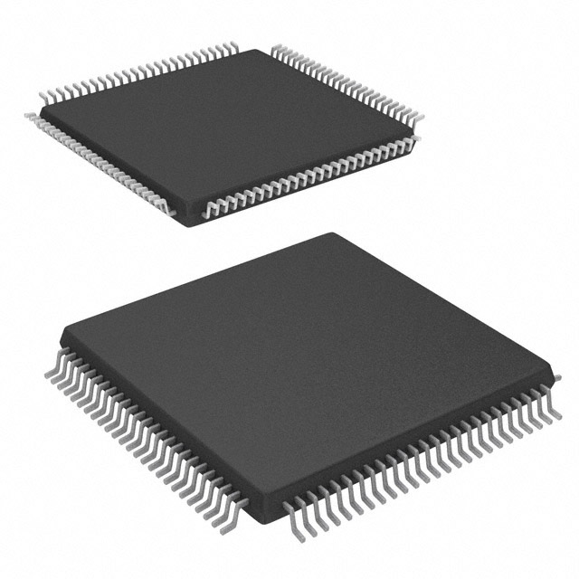
The XC2C256-7VQ100I comes in a VQ100 package, which refers to a quad flat pack with 100 pins.
Essence
The essence of this product lies in its ability to provide reconfigurable logic functionality, allowing designers to implement complex digital circuits with ease.
Packaging/Quantity
The XC2C256-7VQ100I is typically packaged individually and is available in varying quantities depending on the supplier.
Specifications
- Logic Elements: 256
- Flip-Flops: 4,096
- Maximum Frequency: 200 MHz
- I/O Pins: 92
- Operating Voltage: 3.3V
- Operating Temperature Range: -40°C to 85°C
Detailed Pin Configuration
The XC2C256-7VQ100I has a total of 100 pins, each serving a specific purpose. The pin configuration is as follows:
(Pin Number) (Pin Name) - (Function) 1 - GND (Ground) 2 - IO0 - Input/Output Pin 0 3 - IO1 - Input/Output Pin 1 ... 100 - VCC (Power Supply)
Functional Features
- Reconfigurable Logic: The XC2C256-7VQ100I allows users to modify the logic functions according to their requirements.
- JTAG Support: It supports Joint Test Action Group (JTAG) for programming and debugging purposes.
- Embedded Memory: The device includes embedded memory blocks for storing data.
Advantages and Disadvantages
Advantages
- Flexibility: The reconfigurable nature of this PLD enables designers to adapt to changing project requirements.
- Cost-effective: By eliminating the need for custom hardware, the XC2C256-7VQ100I reduces development costs.
- High-performance: With its fast operating speed, it can handle complex digital circuits efficiently.
Disadvantages
- Learning Curve: Utilizing the full potential of this PLD requires a certain level of expertise in digital circuit design.
- Limited I/O Pins: The number of available I/O pins may restrict the complexity of designs that can be implemented.
Working Principles
The XC2C256-7VQ100I operates based on the principles of field-programmable gate arrays (FPGAs). It consists of configurable logic blocks interconnected through programmable interconnects. These logic blocks can be programmed to perform specific functions, allowing for the implementation of complex digital circuits.
Detailed Application Field Plans
The XC2C256-7VQ100I finds applications in various fields, including: - Communication Systems - Industrial Automation - Consumer Electronics - Medical Devices - Automotive Systems
In communication systems, it can be used for protocol conversion, signal processing, and encryption. In industrial automation, it enables control and monitoring of machinery. In consumer electronics, it facilitates the implementation of advanced features in devices such as televisions and smartphones. In medical devices, it can be utilized for data acquisition and processing. In automotive systems, it enables functions like engine control and driver assistance.
Detailed and Complete Alternative Models
- XC2C256-7VQ100C: Similar to XC2C256-7VQ100I but with a different package.
- XC2C256-10PQG208C: A higher-performance variant with increased logic elements and I/O pins.
- XC2C256-4TQ144C: A lower-cost option with reduced logic elements and I/O pins.
These alternative models offer varying features and specifications, allowing designers to choose the most suitable option based on their project requirements.
In conclusion, the XC2C256-7VQ100I is a programmable logic device that provides flexibility, high performance, and low power consumption. Its reconfigurable nature makes it suitable for a wide range of applications in different industries. While it requires expertise in digital circuit design, its advantages outweigh the limitations, making it an excellent choice for complex digital circuit implementation.
Senaraikan 10 soalan dan jawapan biasa yang berkaitan dengan aplikasi XC2C256-7VQ100I dalam penyelesaian teknikal
Sure! Here are 10 common questions and answers related to the application of XC2C256-7VQ100I in technical solutions:
Question: What is XC2C256-7VQ100I?
Answer: XC2C256-7VQ100I is a specific model of CoolRunner-II CPLD (Complex Programmable Logic Device) manufactured by Xilinx.Question: What is the purpose of using XC2C256-7VQ100I in technical solutions?
Answer: XC2C256-7VQ100I is used for implementing digital logic functions, such as data processing, control logic, and interface protocols, in various electronic systems.Question: What are some typical applications of XC2C256-7VQ100I?
Answer: XC2C256-7VQ100I can be found in applications like industrial automation, consumer electronics, telecommunications, automotive systems, and medical devices.Question: How does XC2C256-7VQ100I differ from other CPLDs?
Answer: XC2C256-7VQ100I offers a balance between logic capacity, performance, and power consumption, making it suitable for a wide range of applications.Question: What is the maximum number of user-configurable logic cells in XC2C256-7VQ100I?
Answer: XC2C256-7VQ100I has 256 macrocells or logic cells that can be configured by the user.Question: Can XC2C256-7VQ100I be reprogrammed after it has been configured?
Answer: Yes, XC2C256-7VQ100I supports in-system programming, allowing for reconfiguration without the need for physical replacement.Question: What is the maximum operating frequency of XC2C256-7VQ100I?
Answer: The maximum operating frequency of XC2C256-7VQ100I depends on the specific design and implementation, but it can typically reach several tens or hundreds of megahertz.Question: Does XC2C256-7VQ100I support different I/O voltage levels?
Answer: Yes, XC2C256-7VQ100I supports multiple I/O standards and can be configured to work with various voltage levels, including 3.3V, 2.5V, and 1.8V.Question: Can XC2C256-7VQ100I interface with other digital components or microcontrollers?
Answer: Yes, XC2C256-7VQ100I can interface with other digital components using standard protocols like SPI, I2C, UART, or custom interfaces designed within the CPLD itself.Question: Are there any development tools available for programming XC2C256-7VQ100I?
Answer: Yes, Xilinx provides software tools like ISE Design Suite or Vivado Design Suite that allow users to design, simulate, and program XC2C256-7VQ100I-based solutions.
Please note that these answers are general and may vary depending on the specific requirements and use cases of your technical solution.