

XC2V2000-5FF896I
Product Overview
Category
The XC2V2000-5FF896I belongs to the category of Field Programmable Gate Arrays (FPGAs).
Use
FPGAs are integrated circuits that can be programmed and reprogrammed to perform various digital functions. The XC2V2000-5FF896I is specifically designed for high-performance applications that require complex logic functions.
Characteristics
- High capacity: The XC2V2000-5FF896I has a large number of configurable logic blocks, allowing for the implementation of complex designs.
- Flexibility: FPGAs offer the advantage of being reprogrammable, enabling rapid prototyping and design iterations.
- Parallel processing: FPGAs can execute multiple tasks simultaneously, making them suitable for applications requiring high-speed data processing.
- Low power consumption: The XC2V2000-5FF896I is designed to minimize power consumption while maintaining high performance.
Package
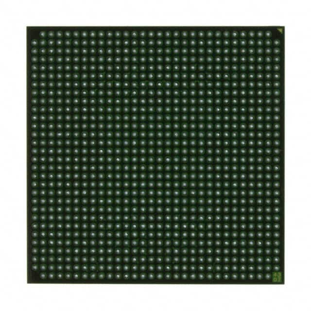
The XC2V2000-5FF896I comes in a FineLine BGA package, which provides a compact form factor and excellent thermal characteristics.
Essence
The essence of the XC2V2000-5FF896I lies in its ability to provide a highly flexible and customizable solution for digital circuit design.
Packaging/Quantity
The XC2V2000-5FF896I is typically packaged individually and is available in various quantities depending on the customer's requirements.
Specifications
- Device type: FPGA
- Family: Virtex-II
- Logic cells: 2,000,000
- Speed grade: -5
- Package: FineLine BGA
- Pin count: 896
- Operating voltage: 1.8V
- Maximum operating frequency: 250 MHz
- I/O standards: LVCMOS, LVTTL, LVDS, HSTL, SSTL
Detailed Pin Configuration
The XC2V2000-5FF896I has 896 pins arranged in a specific configuration. Please refer to the datasheet provided by the manufacturer for detailed pin assignments.
Functional Features
- Configurable logic blocks: The XC2V2000-5FF896I contains a large number of configurable logic blocks that can be programmed to implement various digital functions.
- Block RAM: The device includes dedicated block RAM resources for efficient data storage and retrieval.
- High-speed I/Os: The XC2V2000-5FF896I supports various high-speed I/O standards, enabling seamless integration with external devices.
- Clock management: The FPGA provides flexible clocking options, including phase-locked loops (PLLs) for precise timing control.
- Embedded multipliers: The XC2V2000-5FF896I features embedded multipliers, allowing for efficient implementation of arithmetic operations.
Advantages and Disadvantages
Advantages
- Flexibility: FPGAs offer the advantage of being reprogrammable, allowing for rapid design iterations and customization.
- High performance: The XC2V2000-5FF896I provides a large number of logic cells and high-speed I/Os, enabling the implementation of complex designs.
- Parallel processing: FPGAs can execute multiple tasks simultaneously, making them suitable for applications requiring high-speed data processing.
Disadvantages
- Complexity: Designing and programming FPGAs can be challenging, requiring specialized knowledge and expertise.
- Cost: FPGAs tend to be more expensive compared to other integrated circuits due to their complexity and flexibility.
Working Principles
FPGAs like the XC2V2000-5FF896I consist of an array of configurable logic blocks interconnected through programmable routing resources. These logic blocks can be programmed using a hardware description language (HDL) to implement desired digital functions. The configuration data is stored in internal memory elements and can be reprogrammed as needed.
During operation, the FPGA executes the programmed logic functions in parallel, utilizing the available resources efficiently. Input and output signals are routed through the configurable I/O blocks, allowing for seamless integration with external devices.
Detailed Application Field Plans
The XC2V2000-5FF896I finds applications in various fields, including:
- Telecommunications: FPGAs are used in base stations, network routers, and switches to handle high-speed data processing and protocol conversion.
- Aerospace and Defense: The XC2V2000-5FF896I is suitable for radar systems, avionics, and military communication equipment due to its high performance and flexibility.
- Industrial Automation: FPGAs are utilized in industrial control systems, robotics, and machine vision applications for real-time data processing and control.
- Medical Devices: The XC2V2000-5FF896I can be found in medical imaging equipment, patient monitoring systems, and laboratory instruments, providing high-performance signal processing capabilities.
Senaraikan 10 soalan dan jawapan biasa yang berkaitan dengan aplikasi XC2V2000-5FF896I dalam penyelesaian teknikal
Sure! Here are 10 common questions and answers related to the application of XC2V2000-5FF896I in technical solutions:
Q: What is XC2V2000-5FF896I? A: XC2V2000-5FF896I is a specific model of Field Programmable Gate Array (FPGA) manufactured by Xilinx.
Q: What are the key features of XC2V2000-5FF896I? A: Some key features of XC2V2000-5FF896I include 2 million system gates, 2,048 logic cells, 64 DSP slices, and 80 I/O pins.
Q: What are the typical applications of XC2V2000-5FF896I? A: XC2V2000-5FF896I is commonly used in various technical solutions such as digital signal processing, telecommunications, aerospace, industrial automation, and high-performance computing.
Q: How does XC2V2000-5FF896I differ from other FPGAs? A: XC2V2000-5FF896I stands out due to its large number of system gates, logic cells, DSP slices, and I/O pins, making it suitable for complex and demanding applications.
Q: Can XC2V2000-5FF896I be reprogrammed after deployment? A: Yes, XC2V2000-5FF896I is a field-programmable device, meaning it can be reprogrammed even after being deployed in a system.
Q: What programming languages can be used with XC2V2000-5FF896I? A: XC2V2000-5FF896I can be programmed using Hardware Description Languages (HDLs) such as VHDL or Verilog.
Q: Are there any development tools available for XC2V2000-5FF896I? A: Yes, Xilinx provides development tools like Vivado Design Suite that support XC2V2000-5FF896I and facilitate FPGA design and programming.
Q: Can XC2V2000-5FF896I interface with other components in a system? A: Yes, XC2V2000-5FF896I supports various communication protocols and interfaces like SPI, I2C, UART, Ethernet, and PCIe, allowing it to interact with other system components.
Q: What are the power requirements for XC2V2000-5FF896I? A: XC2V2000-5FF896I typically operates at a voltage range of 1.14V to 1.26V and requires a stable power supply with appropriate current capabilities.
Q: Where can I find more information about XC2V2000-5FF896I? A: You can refer to the official documentation provided by Xilinx, including datasheets, user guides, and application notes, to get detailed information about XC2V2000-5FF896I.