

XC3S1600E-4FG320C
Product Overview
Category
The XC3S1600E-4FG320C belongs to the category of Field Programmable Gate Arrays (FPGAs).
Use
FPGAs are integrated circuits that can be programmed after manufacturing, allowing for flexible and customizable digital logic designs. The XC3S1600E-4FG320C is specifically designed for high-performance applications.
Characteristics
- High capacity: The XC3S1600E-4FG320C has a large number of configurable logic blocks, making it suitable for complex designs.
- Fast performance: It offers high-speed data processing capabilities, enabling efficient execution of complex algorithms.
- Low power consumption: The FPGA is designed to minimize power usage, making it energy-efficient.
- Versatility: The XC3S1600E-4FG320C supports various I/O standards, allowing for seamless integration with different devices.
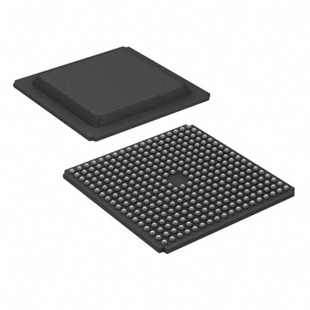
- Robust packaging: It comes in a FG320C package, which provides protection against environmental factors and ensures reliable operation.
Packaging/Quantity
The XC3S1600E-4FG320C is typically packaged individually and is available in various quantities depending on the manufacturer's specifications.
Specifications
- Device type: FPGA
- Family: Spartan-3E
- Logic cells: 1,600
- Maximum frequency: 400 MHz
- Number of I/O pins: 320
- Operating voltage: 1.2V
- Package: FG320C
Detailed Pin Configuration
The XC3S1600E-4FG320C has a total of 320 I/O pins, each serving a specific purpose within the FPGA's design. A detailed pin configuration diagram can be found in the product datasheet provided by the manufacturer.
Functional Features
- Configurable logic blocks: The XC3S1600E-4FG320C offers a large number of logic cells that can be programmed to perform various functions, allowing for complex digital designs.
- Programmable interconnects: The FPGA provides flexible interconnections between logic blocks, enabling efficient communication and data flow within the circuit.
- Embedded memory: It includes dedicated memory blocks that can be used for storing data or implementing lookup tables.
- Clock management: The XC3S1600E-4FG320C supports advanced clocking features, allowing precise timing control for synchronous operations.
Advantages and Disadvantages
Advantages
- Flexibility: FPGAs offer the advantage of reprogrammability, allowing for quick design iterations and customization.
- High performance: The XC3S1600E-4FG320C delivers fast processing speeds, making it suitable for demanding applications.
- Integration: It can interface with various peripheral devices, enabling seamless integration into complex systems.
Disadvantages
- Complexity: Designing for FPGAs requires specialized knowledge and expertise, which may pose a challenge for beginners.
- Cost: FPGAs tend to be more expensive compared to other integrated circuits due to their versatility and programmability.
Working Principles
The XC3S1600E-4FG320C operates based on the principles of configurable logic. It consists of an array of logic cells that can be programmed to implement desired digital functions. These logic cells are interconnected through programmable routing resources, allowing for the creation of complex digital circuits. The FPGA's behavior is determined by the configuration data loaded into its internal memory, which defines the functionality of each logic block and the interconnections between them.
Detailed Application Field Plans
The XC3S1600E-4FG320C finds applications in various fields, including:
- Communications: It can be used in high-speed data transmission systems, such as network routers and switches.
- Signal processing: The FPGA's computational capabilities make it suitable for applications like image and audio processing.
- Industrial automation: It can be employed in control systems, robotics, and machine vision applications.
- Aerospace and defense: FPGAs are utilized in radar systems, avionics, and secure communication systems.
- Medical devices: The XC3S1600E-4FG320C can be integrated into medical imaging equipment and diagnostic devices.
Detailed and Complete Alternative Models
- XC3S500E-4FG320C: A lower-capacity FPGA from the same Spartan-3E family, offering 500 logic cells.
- XC3S2000E-4FG320C: A higher-capacity FPGA with 2,000 logic cells, providing increased performance for complex designs.
- XC6SLX150T-3FGG484C: An alternative FPGA from the newer Spartan-6 family, featuring advanced features and improved performance.
These alternative models offer different capacities and features, allowing users to choose the most suitable FPGA for their specific requirements.
In conclusion, the XC3S1600
Senaraikan 10 soalan dan jawapan biasa yang berkaitan dengan aplikasi XC3S1600E-4FG320C dalam penyelesaian teknikal
Sure! Here are 10 common questions and answers related to the application of XC3S1600E-4FG320C in technical solutions:
Q: What is XC3S1600E-4FG320C? A: XC3S1600E-4FG320C is a field-programmable gate array (FPGA) from Xilinx, which offers high-performance digital logic capabilities for various technical applications.
Q: What are the key features of XC3S1600E-4FG320C? A: Some key features of XC3S1600E-4FG320C include 1,600,000 system gates, 576 Kb of block RAM, 32 DSP slices, and support for various I/O standards.
Q: What are the typical applications of XC3S1600E-4FG320C? A: XC3S1600E-4FG320C can be used in a wide range of applications such as telecommunications, industrial automation, medical devices, aerospace, and defense systems.
Q: How can XC3S1600E-4FG320C be programmed? A: XC3S1600E-4FG320C can be programmed using Xilinx's Vivado Design Suite or ISE Design Suite software tools, which allow users to design and implement their custom logic circuits.
Q: What is the power supply requirement for XC3S1600E-4FG320C? A: XC3S1600E-4FG320C requires a single 1.2V core voltage supply and a separate 2.5V to 3.3V auxiliary voltage supply for configuration and I/O operations.
Q: Can XC3S1600E-4FG320C interface with other devices? A: Yes, XC3S1600E-4FG320C supports various I/O standards such as LVCMOS, LVTTL, LVDS, and differential signaling, allowing it to interface with a wide range of external devices.
Q: What is the maximum operating frequency of XC3S1600E-4FG320C? A: The maximum operating frequency of XC3S1600E-4FG320C depends on the specific design and implementation, but it can typically achieve frequencies in the range of several hundred megahertz (MHz) to a few gigahertz (GHz).
Q: Can XC3S1600E-4FG320C be reprogrammed after deployment? A: Yes, XC3S1600E-4FG320C is a field-programmable device, which means it can be reprogrammed even after it has been deployed in a system, allowing for flexibility and updates.
Q: Are there any development boards available for XC3S1600E-4FG320C? A: Yes, Xilinx offers development boards like the Spartan-6 FPGA SP605 Evaluation Kit, which includes XC3S1600E-4FG320C, allowing users to prototype and test their designs.
Q: Where can I find more information about XC3S1600E-4FG320C? A: You can find more detailed information about XC3S1600E-4FG320C in the official documentation provided by Xilinx, including datasheets, user guides, and application notes.