

XC6VLX365T-3FFG1156C
Product Overview
Category
XC6VLX365T-3FFG1156C belongs to the category of Field Programmable Gate Arrays (FPGAs).
Use
This FPGA is primarily used in digital logic circuits for various applications such as telecommunications, data processing, and embedded systems.
Characteristics
- High-performance FPGA with advanced features
- Large capacity and high-speed processing capabilities
- Flexible and reconfigurable design
- Low power consumption
- Robust and reliable performance
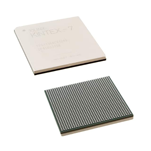
Package
XC6VLX365T-3FFG1156C comes in a compact package that ensures easy integration into electronic systems. The package type is FF1156, which refers to a fine-pitch ball grid array (BGA) package with 1156 balls.
Essence
The essence of XC6VLX365T-3FFG1156C lies in its ability to provide a customizable hardware platform for implementing complex digital designs efficiently.
Packaging/Quantity
This FPGA is typically sold individually and is available in various packaging options, including trays or reels. The exact quantity per package may vary depending on the supplier.
Specifications
- Logic Cells: 362,080
- Flip-Flops: 724,160
- Block RAM: 4,860 Kb
- DSP Slices: 1,920
- Maximum I/O Pins: 500
- Operating Voltage: 1.2V
- Maximum Operating Frequency: 550 MHz
- Configuration Memory: 36 Mb
Detailed Pin Configuration
The detailed pin configuration of XC6VLX365T-3FFG1156C can be found in the product datasheet provided by the manufacturer. It includes information about input/output pins, power supply pins, clock pins, and other specialized pins.
Functional Features
- High-speed serial connectivity
- Embedded hard IP cores for various functions (e.g., memory controllers, Ethernet MAC)
- Advanced DSP capabilities for signal processing applications
- Configurable I/O standards and voltage levels
- On-chip power management features
Advantages and Disadvantages
Advantages
- Versatile and flexible design options
- High-performance processing capabilities
- Low power consumption compared to alternative solutions
- Extensive library of pre-designed IP cores available
- Easy integration into existing systems
Disadvantages
- Higher cost compared to traditional ASICs or microcontrollers
- Steeper learning curve for beginners due to the complexity of FPGA programming
- Limited availability of open-source tools and resources
Working Principles
XC6VLX365T-3FFG1156C operates based on the principles of reconfigurable computing. It consists of a matrix of configurable logic blocks interconnected through programmable routing resources. The device can be programmed to implement desired digital logic circuits by configuring the interconnections and functionality of these logic blocks.
Detailed Application Field Plans
XC6VLX365T-3FFG1156C finds applications in various fields, including:
- Telecommunications: Used in base stations, network switches, and routers for high-speed data processing and protocol handling.
- Aerospace and Defense: Employed in radar systems, avionics, and military communication equipment for their high-performance and reliability.
- Industrial Automation: Utilized in control systems, motor drives, and robotics for real-time processing and precise control.
- Medical Devices: Integrated into medical imaging systems, patient monitoring devices, and laboratory equipment for data acquisition and processing.
- Automotive: Applied in advanced driver-assistance systems (ADAS), infotainment systems, and engine control units (ECUs) for enhanced functionality and performance.
Detailed and Complete Alternative Models
- XC7A100T-1FGG484C: A lower-cost alternative with similar capabilities but a smaller logic capacity.
- XC7K325T-2FFG900C: A higher-end alternative with increased logic capacity and additional features such as high-speed transceivers.
- XC6SLX9-2FTG256C: A compact alternative suitable for low-power applications with moderate logic requirements.
These alternative models provide options based on specific project requirements, budget constraints, and performance needs.
In conclusion, XC6VLX365T-3FFG1156C is a high-performance FPGA that offers flexibility, reliability, and advanced features for various digital logic applications. Its extensive range of specifications, functional features, and application field plans make it a versatile choice for designers seeking customizable hardware solutions.
Senaraikan 10 soalan dan jawapan biasa yang berkaitan dengan aplikasi XC6VLX365T-3FFG1156C dalam penyelesaian teknikal
Sure! Here are 10 common questions and answers related to the application of XC6VLX365T-3FFG1156C in technical solutions:
Q: What is XC6VLX365T-3FFG1156C? A: XC6VLX365T-3FFG1156C is a field-programmable gate array (FPGA) from Xilinx, which offers high-performance processing capabilities for various technical applications.
Q: What are the key features of XC6VLX365T-3FFG1156C? A: Some key features include a large number of logic cells, high-speed serial transceivers, embedded memory blocks, DSP slices, and support for various communication protocols.
Q: What technical solutions can XC6VLX365T-3FFG1156C be used for? A: XC6VLX365T-3FFG1156C can be used in a wide range of applications such as telecommunications, networking, aerospace, defense, industrial automation, and scientific research.
Q: How does XC6VLX365T-3FFG1156C provide high performance? A: XC6VLX365T-3FFG1156C achieves high performance through its advanced architecture, parallel processing capabilities, and optimized routing resources.
Q: Can XC6VLX365T-3FFG1156C be programmed using industry-standard design tools? A: Yes, XC6VLX365T-3FFG1156C can be programmed using Xilinx's Vivado Design Suite, which is an industry-standard toolset for FPGA development.
Q: Does XC6VLX365T-3FFG1156C support high-speed serial communication? A: Yes, XC6VLX365T-3FFG1156C supports high-speed serial communication protocols such as PCIe, Ethernet, USB, and SATA.
Q: Can XC6VLX365T-3FFG1156C be used for real-time signal processing? A: Yes, XC6VLX365T-3FFG1156C's DSP slices and embedded memory blocks make it suitable for real-time signal processing applications like image and video processing.
Q: What is the power consumption of XC6VLX365T-3FFG1156C? A: The power consumption of XC6VLX365T-3FFG1156C depends on the specific application and configuration but typically ranges from a few watts to tens of watts.
Q: Can XC6VLX365T-3FFG1156C be used in safety-critical applications? A: Yes, XC6VLX365T-3FFG1156C can be used in safety-critical applications with appropriate design techniques and adherence to relevant industry standards.
Q: Are there any development boards or evaluation kits available for XC6VLX365T-3FFG1156C? A: Yes, Xilinx offers development boards and evaluation kits specifically designed for XC6VLX365T-3FFG1156C, which provide a platform for prototyping and testing different applications.
Please note that the answers provided here are general and may vary depending on the specific requirements and use cases of XC6VLX365T-3FFG1156C in technical solutions.