

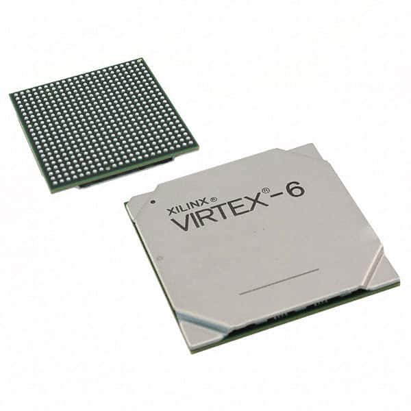
XC6VLX75T-L1FFG784I
Product Overview
Category
The XC6VLX75T-L1FFG784I belongs to the category of Field-Programmable Gate Arrays (FPGAs).
Use
FPGAs are integrated circuits that can be programmed and reprogrammed to perform various digital functions. The XC6VLX75T-L1FFG784I is specifically designed for high-performance applications.
Characteristics
- High-performance FPGA
- Programmable and reprogrammable
- Suitable for complex digital designs
- Offers flexibility and customization options
Package
The XC6VLX75T-L1FFG784I comes in a specific package known as the Flip-Chip Fine-Pitch Ball Grid Array (FFG784). This package provides excellent thermal performance and allows for easy integration onto printed circuit boards.
Essence
The essence of the XC6VLX75T-L1FFG784I lies in its ability to provide a highly configurable and customizable solution for digital design requirements.
Packaging/Quantity
The XC6VLX75T-L1FFG784I is typically packaged individually and is available in various quantities depending on the manufacturer's specifications.
Specifications
- Logic Cells: 75,000
- Slices: 4,800
- DSP48E1 Slices: 240
- Block RAM: 3,600 Kbits
- Maximum I/O Pins: 784
- Clock Management Tiles: 8
- Operating Voltage: 1.2V
- Speed Grade: L1
Detailed Pin Configuration
The detailed pin configuration of the XC6VLX75T-L1FFG784I can be found in the product datasheet provided by the manufacturer. It includes information about each pin's functionality, voltage levels, and recommended usage.
Functional Features
- High-performance processing capabilities
- Configurable logic cells for custom designs
- Dedicated DSP slices for efficient signal processing
- Abundant memory resources for data storage and retrieval
- Flexible clock management tiles for precise timing control
Advantages and Disadvantages
Advantages
- High level of customization and flexibility
- Ability to implement complex digital designs
- Fast development time due to reprogrammability
- Suitable for a wide range of applications
- Availability of comprehensive design tools and support
Disadvantages
- Higher power consumption compared to fixed-function ASICs
- Limited performance compared to specialized hardware
- Higher cost per unit compared to mass-produced integrated circuits
Working Principles
The XC6VLX75T-L1FFG784I operates based on the principles of FPGA technology. It consists of configurable logic blocks, interconnect resources, and various other components that can be programmed to perform specific digital functions. The device is programmed using Hardware Description Languages (HDL) such as VHDL or Verilog.
Detailed Application Field Plans
The XC6VLX75T-L1FFG784I finds applications in various fields, including:
- Telecommunications: Used in high-speed data transmission systems and network infrastructure equipment.
- Aerospace and Defense: Employed in radar systems, avionics, and military communication devices.
- Industrial Automation: Utilized in programmable logic controllers (PLCs) and industrial control systems.
- Medical Electronics: Applied in medical imaging devices, patient monitoring systems, and diagnostic equipment.
- Automotive: Used in advanced driver-assistance systems (ADAS), infotainment systems, and engine control units (ECUs).
Detailed and Complete Alternative Models
- XC7A100T-1FGG484C: A similar FPGA from Xilinx with enhanced performance and higher logic capacity.
- EP4CE115F29C7: An FPGA from Altera (now Intel) offering comparable features and functionality.
- Lattice ECP5-85: A low-power FPGA with advanced DSP capabilities suitable for power-constrained applications.
These alternative models provide similar functionalities to the XC6VLX75T-L1FFG784I and can be considered based on specific project requirements.
In conclusion, the XC6VLX75T-L1FFG784I is a high-performance FPGA that offers flexibility, customization options, and a wide range of applications. Its configurable nature, abundant resources, and comprehensive design tools make it an ideal choice for complex digital designs. However, it is important to consider its power consumption, performance limitations, and cost when selecting this FPGA for a particular project.
Senaraikan 10 soalan dan jawapan biasa yang berkaitan dengan aplikasi XC6VLX75T-L1FFG784I dalam penyelesaian teknikal
Sure! Here are 10 common questions and answers related to the application of XC6VLX75T-L1FFG784I in technical solutions:
Q1: What is XC6VLX75T-L1FFG784I? A1: XC6VLX75T-L1FFG784I is a specific model of Xilinx Virtex-6 FPGA (Field-Programmable Gate Array) that offers high-performance processing capabilities for various technical applications.
Q2: What are the key features of XC6VLX75T-L1FFG784I? A2: Some key features of XC6VLX75T-L1FFG784I include a large number of logic cells, high-speed serial transceivers, embedded memory blocks, DSP slices, and support for various communication protocols.
Q3: What are the typical applications of XC6VLX75T-L1FFG784I? A3: XC6VLX75T-L1FFG784I can be used in a wide range of applications such as aerospace and defense systems, telecommunications equipment, industrial automation, medical devices, and high-performance computing.
Q4: How can XC6VLX75T-L1FFG784I be programmed? A4: XC6VLX75T-L1FFG784I can be programmed using Xilinx's Vivado Design Suite or ISE Design Suite. These software tools allow users to design, simulate, and program the FPGA according to their specific requirements.
Q5: Can XC6VLX75T-L1FFG784I be reprogrammed after deployment? A5: Yes, XC6VLX75T-L1FFG784I is a reprogrammable FPGA, which means that it can be reconfigured with new designs even after it has been deployed in a system.
Q6: What are the advantages of using XC6VLX75T-L1FFG784I in technical solutions? A6: Some advantages of using XC6VLX75T-L1FFG784I include its high processing power, flexibility, and ability to handle complex algorithms. It also offers low latency and high bandwidth communication capabilities.
Q7: Are there any limitations or considerations when using XC6VLX75T-L1FFG784I? A7: One consideration is that XC6VLX75T-L1FFG784I consumes a significant amount of power, so proper power management and cooling should be implemented. Additionally, it may require expertise in FPGA design and programming.
Q8: Can XC6VLX75T-L1FFG784I interface with other components or devices? A8: Yes, XC6VLX75T-L1FFG784I supports various interfaces such as PCIe, Ethernet, USB, SPI, I2C, and more. This allows it to communicate with other components or devices in a system.
Q9: Is XC6VLX75T-L1FFG784I suitable for real-time applications? A9: Yes, XC6VLX75T-L1FFG784I can be used in real-time applications due to its high-speed processing capabilities and support for parallel computing.
Q10: Where can I find additional resources or support for XC6VLX75T-L1FFG784I? A10: Xilinx provides comprehensive documentation, application notes, reference designs, and technical support through their website and community forums. You can also consult Xilinx's user guides and datasheets for detailed information on XC6VLX75T-L1FFG784I.