

XC7A35T-L1CSG325I
Product Overview
Category
The XC7A35T-L1CSG325I belongs to the category of Field-Programmable Gate Arrays (FPGAs).
Use
FPGAs are integrated circuits that can be programmed and reprogrammed to perform various digital functions. The XC7A35T-L1CSG325I is specifically designed for applications that require high-performance processing, such as data centers, telecommunications, industrial automation, and scientific research.
Characteristics
- High-performance FPGA with advanced programmable logic capabilities.
- Offers a wide range of configurable resources, including logic cells, memory blocks, and input/output interfaces.
- Supports complex digital designs and algorithms.
- Provides flexibility in system design and customization.
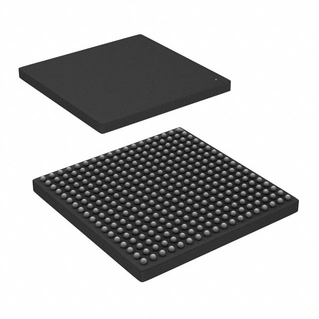
Package
The XC7A35T-L1CSG325I comes in a compact and durable package, ensuring easy integration into electronic systems. The package type is L1CSG325I.
Essence
The essence of the XC7A35T-L1CSG325I lies in its ability to provide a highly flexible and customizable solution for digital processing tasks. It allows designers to implement complex algorithms and designs efficiently, enabling faster time-to-market and improved system performance.
Packaging/Quantity
The XC7A35T-L1CSG325I is typically packaged in trays or reels, depending on the manufacturer's specifications. The quantity per package may vary, but it is commonly available in quantities suitable for both prototyping and production purposes.
Specifications
- Logic Cells: 33,280
- Block RAM: 1,800 Kbits
- DSP Slices: 90
- Maximum I/O Pins: 325
- Operating Voltage: 1.2V
- Maximum Operating Frequency: 550 MHz
- Configuration Memory: 4 Mb
- Package Type: L1CSG325I
Detailed Pin Configuration
The XC7A35T-L1CSG325I has a total of 325 I/O pins, which are configurable for various purposes. The pin configuration is as follows:
- Pin 1: VCCINT
- Pin 2: GND
- Pin 3: IOL1PT0L_15
- Pin 4: IOL1NT0L_15
- ...
- Pin 324: IOL18PT3L_34
- Pin 325: IOL18NT3L_34
For a complete and detailed pin configuration diagram, please refer to the manufacturer's datasheet.
Functional Features
The XC7A35T-L1CSG325I offers several functional features that make it a versatile FPGA solution:
- High Logic Capacity: With 33,280 logic cells, it can accommodate complex digital designs and algorithms.
- Flexible I/O Interfaces: The FPGA provides 325 I/O pins, allowing for seamless integration with external devices and systems.
- Advanced Memory Resources: The 1,800 Kbits of block RAM enable efficient data storage and retrieval.
- DSP Slices: The 90 dedicated DSP slices offer high-performance signal processing capabilities.
- Configurability: The FPGA can be easily programmed and reprogrammed to adapt to changing system requirements.
Advantages and Disadvantages
Advantages
- High-performance processing capabilities.
- Flexibility in system design and customization.
- Efficient utilization of resources.
- Versatile I/O interfaces for seamless integration.
- Support for complex digital designs and algorithms.
Disadvantages
- Steep learning curve for beginners due to the complexity of FPGA programming.
- Higher power consumption compared to other digital processing solutions.
- Relatively higher cost compared to microcontrollers or application-specific integrated circuits (ASICs).
Working Principles
The XC7A35T-L1CSG325I operates based on the principles of reconfigurable logic. It consists of a matrix of configurable logic cells and programmable interconnects. The logic cells can be programmed to perform various digital functions, such as arithmetic operations, data storage, and control logic. The interconnects allow for the routing of signals between different logic cells, enabling the implementation of complex digital designs.
The FPGA is programmed using Hardware Description Languages (HDLs) like VHDL or Verilog. The HDL code describes the desired functionality of the FPGA, which is then synthesized and implemented onto the device using specialized software tools provided by the FPGA manufacturer.
Detailed Application Field Plans
The XC7A35T-L1CSG325I finds applications in various fields that require high-performance digital processing capabilities. Some detailed application field plans include:
- Data Centers: The FPGA can be used for accelerating data processing tasks, such as encryption, compression, and database operations.
- Telecommunications: It can be employed in network routers, switches, and base stations to handle high-speed data
Senaraikan 10 soalan dan jawapan biasa yang berkaitan dengan aplikasi XC7A35T-L1CSG325I dalam penyelesaian teknikal
Sure! Here are 10 common questions and answers related to the application of XC7A35T-L1CSG325I in technical solutions:
Q1: What is XC7A35T-L1CSG325I? A1: XC7A35T-L1CSG325I is a specific model of Xilinx Artix-7 FPGA (Field-Programmable Gate Array) that offers a range of features and capabilities for implementing digital logic designs.
Q2: What are the key features of XC7A35T-L1CSG325I? A2: Some key features of XC7A35T-L1CSG325I include 33,280 logic cells, 1,800 Kbits of block RAM, 90 DSP slices, and support for various I/O standards.
Q3: What are the typical applications of XC7A35T-L1CSG325I? A3: XC7A35T-L1CSG325I can be used in a wide range of applications such as industrial automation, automotive electronics, medical devices, communication systems, and more.
Q4: How can XC7A35T-L1CSG325I be programmed? A4: XC7A35T-L1CSG325I can be programmed using Xilinx's Vivado Design Suite, which provides a comprehensive development environment for designing, simulating, and programming FPGAs.
Q5: What are the power requirements for XC7A35T-L1CSG325I? A5: The power requirements for XC7A35T-L1CSG325I depend on the specific design and configuration. It typically operates at a voltage range of 0.95V to 1.05V.
Q6: Can XC7A35T-L1CSG325I interface with other components or devices? A6: Yes, XC7A35T-L1CSG325I supports various I/O standards and can interface with other components or devices such as sensors, memory modules, communication interfaces, and more.
Q7: Can XC7A35T-L1CSG325I be used for real-time processing? A7: Yes, XC7A35T-L1CSG325I is capable of real-time processing due to its high-speed logic cells and DSP slices, making it suitable for applications that require fast data processing.
Q8: What are the advantages of using XC7A35T-L1CSG325I in technical solutions? A8: Some advantages of using XC7A35T-L1CSG325I include its flexibility, reconfigurability, high-performance capabilities, and ability to implement complex digital logic designs.
Q9: Are there any limitations or considerations when using XC7A35T-L1CSG325I? A9: Some considerations include power consumption, thermal management, and the need for expertise in FPGA design and programming. Additionally, the available resources may limit the complexity of designs.
Q10: Where can I find additional resources or support for XC7A35T-L1CSG325I? A10: Xilinx provides comprehensive documentation, application notes, reference designs, and technical support through their website and community forums.