

XC7S25-2FTGB196C
Product Overview
Category
XC7S25-2FTGB196C belongs to the category of Field Programmable Gate Arrays (FPGAs).
Use
This product is primarily used in digital logic circuits, where it allows users to configure and reconfigure the circuitry according to their specific requirements.
Characteristics
- High flexibility: The XC7S25-2FTGB196C offers a high degree of flexibility as it can be programmed and reprogrammed multiple times.
- High performance: It provides fast processing speeds and efficient execution of complex algorithms.
- Low power consumption: This FPGA consumes relatively low power compared to other similar devices.
- Large capacity: With a capacity of 25,000 logic cells, it can handle a wide range of applications.
- Versatile I/O options: The XC7S25-2FTGB196C supports various input/output standards, making it compatible with different interfaces.
- Robust packaging: It comes in a compact and durable package, ensuring protection during handling and installation.
Packaging/Quantity
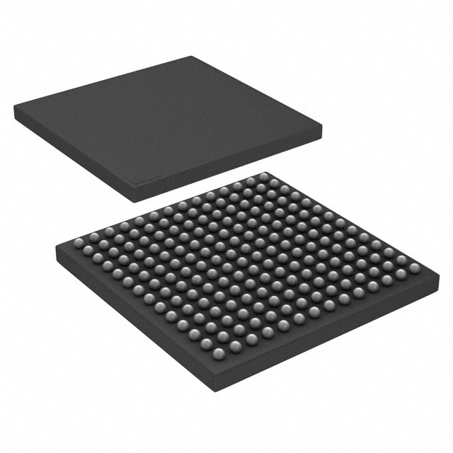
The XC7S25-2FTGB196C is typically packaged in a plastic ball grid array (BGA) package. Each package contains one unit of the FPGA.
Specifications
- Logic Cells: 25,000
- Flip-Flops: 50,000
- Block RAM: 1,800 Kbits
- DSP Slices: 80
- Maximum Frequency: 500 MHz
- Operating Voltage: 1.2V
- Package Type: BGA
- Package Pins: 196
- Temperature Range: -40°C to +100°C
Detailed Pin Configuration
The XC7S25-2FTGB196C has a total of 196 pins. These pins are assigned for various purposes such as power supply, configuration, input/output, and clock signals. A detailed pin configuration diagram can be found in the product datasheet.
Functional Features
- Configurable Logic Blocks (CLBs): The XC7S25-2FTGB196C consists of multiple CLBs that can be programmed to implement various logic functions.
- Programmable Interconnects: It offers a flexible interconnect structure that allows users to establish connections between different logic elements.
- Embedded Memory: This FPGA includes dedicated memory blocks that can be used for storing data or implementing complex algorithms.
- Clock Management: It provides built-in clock management resources, enabling precise control over timing requirements.
- High-Speed Serial Transceivers: The XC7S25-2FTGB196C supports high-speed serial communication protocols, facilitating data transfer at high rates.
Advantages and Disadvantages
Advantages
- Flexibility: The ability to reconfigure the circuitry makes it suitable for prototyping and development stages.
- High Performance: It offers fast processing speeds and efficient execution of complex algorithms.
- Low Power Consumption: The XC7S25-2FTGB196C consumes relatively low power, making it energy-efficient.
- Versatility: With support for various I/O standards, it can interface with a wide range of devices.
Disadvantages
- Complexity: Programming an FPGA requires specialized knowledge and expertise.
- Cost: FPGAs can be more expensive compared to other integrated circuits.
- Limited Scalability: The capacity of an FPGA is fixed, which may restrict its use in applications requiring extensive resources.
Working Principles
The XC7S25-2FTGB196C operates based on the principles of digital logic design. It consists of configurable logic blocks (CLBs) interconnected through programmable routing resources. These CLBs can be programmed to implement desired logic functions, allowing users to create custom digital circuits. The FPGA's functionality is determined by the configuration data loaded into it, which can be modified as needed.
Detailed Application Field Plans
The XC7S25-2FTGB196C finds applications in various fields, including:
- Communications: It can be used for implementing communication protocols, signal processing, and encryption algorithms.
- Industrial Automation: The FPGA's flexibility makes it suitable for controlling and monitoring complex industrial processes.
- Aerospace and Defense: It is utilized in radar systems, avionics, and military-grade communication equipment.
- Medical Devices: FPGAs are employed in medical imaging, patient monitoring, and diagnostic equipment.
- Automotive: They are used in advanced driver-assistance systems (ADAS), engine control units (ECUs), and infotainment systems.
Detailed and Complete Alternative Models
- XC7S50-2FTGB196C: This model offers a higher logic cell count and increased performance compared to the XC7S25-2FTGB196C.
- XC7A15T-1FTGB196C: A lower-cost alternative with fewer logic cells but suitable for less demanding applications.
- XC7K160T
Senaraikan 10 soalan dan jawapan biasa yang berkaitan dengan aplikasi XC7S25-2FTGB196C dalam penyelesaian teknikal
Sure! Here are 10 common questions and answers related to the application of XC7S25-2FTGB196C in technical solutions:
Q: What is XC7S25-2FTGB196C? A: XC7S25-2FTGB196C is a specific model of Xilinx Spartan-7 FPGA (Field-Programmable Gate Array) with 25,000 logic cells.
Q: What are the key features of XC7S25-2FTGB196C? A: Some key features include low power consumption, high-performance processing, integrated memory blocks, and support for various I/O standards.
Q: What are the typical applications of XC7S25-2FTGB196C? A: XC7S25-2FTGB196C is commonly used in applications such as industrial automation, automotive electronics, communication systems, and embedded computing.
Q: How can XC7S25-2FTGB196C be programmed? A: XC7S25-2FTGB196C can be programmed using Xilinx's Vivado Design Suite, which provides a graphical interface and HDL (Hardware Description Language) support.
Q: What is the maximum operating frequency of XC7S25-2FTGB196C? A: The maximum operating frequency of XC7S25-2FTGB196C depends on the specific design and implementation, but it can typically reach several hundred megahertz.
Q: Can XC7S25-2FTGB196C interface with other components or devices? A: Yes, XC7S25-2FTGB196C supports various I/O standards, including LVCMOS, LVTTL, LVDS, and differential signaling, allowing it to interface with a wide range of components and devices.
Q: What is the power supply requirement for XC7S25-2FTGB196C? A: XC7S25-2FTGB196C requires a single 1.2V core voltage supply and a separate 3.3V auxiliary supply for configuration and I/O operations.
Q: Can XC7S25-2FTGB196C be used in safety-critical applications? A: Yes, XC7S25-2FTGB196C can be used in safety-critical applications with appropriate design considerations and adherence to relevant industry standards.
Q: Are there any development boards or evaluation kits available for XC7S25-2FTGB196C? A: Yes, Xilinx offers development boards and evaluation kits specifically designed for XC7S25-2FTGB196C, providing a convenient platform for prototyping and testing.
Q: Where can I find more information about XC7S25-2FTGB196C and its technical specifications? A: You can refer to the official documentation provided by Xilinx, including datasheets, user guides, and application notes, which are available on their website.