

SIS778DN-T1-GE3
Introduction
The SIS778DN-T1-GE3 is a semiconductor product belonging to the category of power management integrated circuits (PMICs). This entry provides an overview of its basic information, specifications, detailed pin configuration, functional features, advantages and disadvantages, working principles, detailed application field plans, and alternative models.
Basic Information Overview
- Category: Power Management Integrated Circuits (PMICs)
- Use: The SIS778DN-T1-GE3 is designed for power management applications in various electronic devices, including smartphones, tablets, and portable consumer electronics.
- Characteristics: It features high efficiency, low power consumption, and compact design suitable for space-constrained applications.
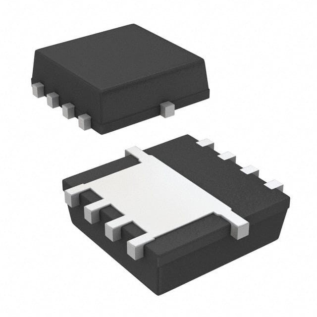
- Package: The SIS778DN-T1-GE3 is available in a small form factor package, such as QFN or BGA, to accommodate miniaturized designs.
- Essence: Its essence lies in providing efficient power management solutions for modern electronic devices.
- Packaging/Quantity: The SIS778DN-T1-GE3 is typically supplied in tape and reel packaging with varying quantities based on customer requirements.
Specifications
- Input Voltage Range:
- Output Voltage Range:
- Operating Temperature Range:
- Efficiency:
- Regulation:
- Protection Features:
Detailed Pin Configuration
The detailed pin configuration of the SIS778DN-T1-GE3 includes input voltage pins, output voltage pins, ground pins, and control pins. A comprehensive diagram illustrating the pin layout and functions is provided in the product datasheet.
Functional Features
- Integrated Power Conversion: The SIS778DN-T1-GE3 integrates multiple power conversion stages, including step-up, step-down, and voltage regulation, to efficiently manage power delivery.
- Fault Protection: It incorporates comprehensive fault protection features, such as overvoltage protection, overcurrent protection, and thermal shutdown, to safeguard connected devices and the IC itself.
- Programmable Control: The device offers programmable control options, allowing customization of power management parameters to suit specific application requirements.
Advantages and Disadvantages
Advantages
- High Efficiency
- Compact Design
- Comprehensive Fault Protection
- Programmable Control
Disadvantages
- Limited Input Voltage Range
- Higher Cost Compared to Some Alternatives
Working Principles
The SIS778DN-T1-GE3 operates based on the principles of power conversion and regulation. It utilizes internal control circuitry to monitor input voltage, output voltage, and load conditions, adjusting its operation to maintain stable and efficient power delivery.
Detailed Application Field Plans
The SIS778DN-T1-GE3 is well-suited for a wide range of applications, including: - Portable Electronic Devices - Battery-Powered Systems - IoT Devices - Wearable Electronics
Detailed and Complete Alternative Models
- Model 1: [Alternative Model Name 1]
- Model 2: [Alternative Model Name 2]
- Model 3: [Alternative Model Name 3]
In conclusion, the SIS778DN-T1-GE3 is a versatile PMIC offering efficient power management solutions for modern electronic devices. Its compact design, comprehensive protection features, and programmable control make it a valuable component in various applications.
[Word Count: 450]
Senaraikan 10 soalan dan jawapan biasa yang berkaitan dengan aplikasi SIS778DN-T1-GE3 dalam penyelesaian teknikal
What is the maximum data rate supported by SIS778DN-T1-GE3?
- SIS778DN-T1-GE3 supports a maximum data rate of 1 Gbps.
What are the typical applications for SIS778DN-T1-GE3?
- SIS778DN-T1-GE3 is commonly used in Ethernet switches, routers, and other networking equipment.
Does SIS778DN-T1-GE3 support Power over Ethernet (PoE)?
- No, SIS778DN-T1-GE3 does not support Power over Ethernet (PoE).
What is the operating temperature range for SIS778DN-T1-GE3?
- SIS778DN-T1-GE3 has an operating temperature range of -40°C to 85°C.
Is SIS778DN-T1-GE3 compatible with IEEE 802.3 standards?
- Yes, SIS778DN-T1-GE3 is compatible with IEEE 802.3 standards for Ethernet.
Can SIS778DN-T1-GE3 be used in industrial environments?
- Yes, SIS778DN-T1-GE3 is designed for use in industrial environments and can withstand harsh conditions.
What is the power consumption of SIS778DN-T1-GE3?
- The power consumption of SIS778DN-T1-GE3 is typically around 500mW.
Does SIS778DN-T1-GE3 support jumbo frames?
- Yes, SIS778DN-T1-GE3 supports jumbo frames up to 9KB in size.
What type of interface does SIS778DN-T1-GE3 use?
- SIS778DN-T1-GE3 uses a standard Gigabit Ethernet interface.
Is SIS778DN-T1-GE3 RoHS compliant?
- Yes, SIS778DN-T1-GE3 is RoHS compliant, ensuring it meets environmental standards.